Continue to Site

Welcome to EDAboard.com

Welcome to our site! EDAboard.com is an international Electronics Discussion Forum focused on EDA software, circuits, schematics, books, theory, papers, asic, pld, 8051, DSP, Network, RF, Analog Design, PCB, Service Manuals... and a whole lot more! To participate you need to register. Registration is free. Click here to register now.

IGBT always boom during load testing!

Status
Not open for further replies.

deJong

Member level 1
Member level 1
Joined
Feb 14, 2015
Messages
33
Helped
0
Reputation
0
Reaction score
0
Trophy points
6
Visit site
Activity points
227
Hello Electronics Enthusiasts!

I'm trying to solve this SMPS unit of mine that keep on blowing my IGBT component. It will kill the unit for less than two minutes of full load testing. Here is the unit:
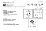
IGBT.jpg
Power-up without load is perfectly fine.
schematic to follow....

Any idea what caused this component to fail? I've monitor the input current drawn by the SMPS and it's very high (more than 10A). It should not go up to 8.5A. Output is also stable during power up at 600V 1.6A until the PS dies.

Thanks!
-deJong
 

im sorry but I don't know the dead time of this design
How about determing it by a measurement?

Seriously speaking, I have little confidence that the transformer circuit will produce acceptable gate waveforms. I may be corrected by a measurement that prove their correctness. Or as a substitute a transformer specification along with the driver circuit.
 

I will try that measurement later FvM because I will be needing an o'scope. For more info, this supply used to have a MOSFET, instead of that IGBT for faster switching and higher functional rating. Not sure exactly what MOSFET.

For the transformer, I think it's all good. But let me verify that later.

My schematic have a resistor already, do I need another one? Could you please explain further why I need it biswaIITH?
What is the current limitting resistor value??
 

For the transformer, I think it's all good. But let me verify that later.
I didn't mean that the transformer is bad. I mean that it's difficult to generate a suitable control signal with this circuit, it's quality will depend on many parameters. Transformer main and leakage inductance are important, also gate capacitance and driver characteristic. Finally the gate voltage varies with duty cycle. Changing the MOSFET against an IGBT can matter a lot.
 

here is the snapshot of the heatsink used Anna Conda
image.jpg
should be good enough
 

OK to fault find your circuit we need the complete circuit with values and freq of operation, also there is a classic problem with the simple way you are driving the igbt's with the gate drive Tx, when you turn on the bottom device the dv/dt on the emitter of the top device will cause it to turn on briefly, this can overheat and kill the top device, you'll need an isolated scope on the top G-S to observe this.
 
may I know what factors that matters FvM?

- - - Updated - - -

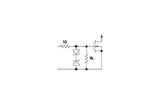
biswaIITH, is this ok?
1kGS.jpg
 

The above ckt will certainly help, how fast (in V/uS) does the drain of the bottom device go down when you turn it on? (e.g. 300V in 50nS?)
You might have to increase the 10 ohm res above (to 220 ohm for example, and incr the 1k to 2k2) to give you slower turn on to stop the induced turn on of the other device. You can put a back diode across the 220 ohm to keep the turn off speed high.
 
  • Like
Reactions: deJong

    deJong

    Points: 2
    Helpful Answer Positive Rating
this is using PWM UC3524, F=1.18/RtCt
Rt=866 Ohms
Ct=0.01uF
therefore F=136.26kHz
 

That seems quite high for an IGBT, but what may be causing a major difference is the gate capacitance. If it is wildly different to that of the Mosfet then you could be hitting a resonance in your gate circuit. Can you scope your gate emitter waveform?

Rob.
 

Even 68kHz might be on the high side for these devices, if switching more than 10A, due to their switching losses and high-ish on drop...
 
@Anna Conda the circuit between PWM IC and IGBT gates is a driver UC3706
 

Status
Not open for further replies.

Similar threads

Part and Inventory Search

Welcome to EDABoard.com

Sponsor

Back
Top