Continue to Site

Welcome to EDAboard.com

Welcome to our site! EDAboard.com is an international Electronics Discussion Forum focused on EDA software, circuits, schematics, books, theory, papers, asic, pld, 8051, DSP, Network, RF, Analog Design, PCB, Service Manuals... and a whole lot more! To participate you need to register. Registration is free. Click here to register now.

Ideal Current Mode Class D (CMCD) question

Status
Not open for further replies.

pYrana13

Junior Member level 1
Joined
Nov 29, 2009
Messages
16
Helped
0
Reputation
0
Reaction score
0
Trophy points
1,281
Activity points
1,407
Hi all,

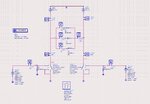
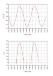
I am designing this CMCD-PA using Agilent ADS. I would like to know, why did the voltage at output load (R4) form a half sinusoidal shape?
Shouldn't it be a full sinusoidal waveform, similar to the current at R4??

You can refer to my schematic and the output in the attachment below.

TQ
 

Attachments

  • Schematic ideal CMCD.JPG
    Schematic ideal CMCD.JPG
    194.3 KB · Views: 147
  • Output Current and Voltage at Load.JPG
    Output Current and Voltage at Load.JPG
    57.9 KB · Views: 135

The "voltage at the output load" is also the voltage at the output transistor. It's hold at zero while the switch is closed by nature of the circuit, so the flat bottom line isn't surprizing.
 
Each switch has a half sine wave shape on it, the voltage appearing across the load will thus be a full sine wave.
 
Status
Not open for further replies.

Part and Inventory Search

Welcome to EDABoard.com

Sponsor

Back
Top