Continue to Site

Welcome to EDAboard.com

Welcome to our site! EDAboard.com is an international Electronics Discussion Forum focused on EDA software, circuits, schematics, books, theory, papers, asic, pld, 8051, DSP, Network, RF, Analog Design, PCB, Service Manuals... and a whole lot more! To participate you need to register. Registration is free. Click here to register now.

How to use MOSFET as a switch to introduce a capacitor into a LC tank in VCO?

Status
Not open for further replies.

Alex Liao

Member level 4
Joined
Apr 8, 2013
Messages
75
Helped
2
Reputation
4
Reaction score
2
Trophy points
1,288
Activity points
1,991
Hi guys,

In my VCO design, if I introduce a fixed capacitance, Cap_fix into the C tank, it works fine and give me the target frequency I want. If I disconnect this path (in parallel with the total C) to disable the introduction of this Cap_fix, it gives me higher frequency and it is reasonable as it follows:
w = 1/sqrt(C*L).

But if I want to implement this on/off feature using a MOSFET it does not work.
It always generates strange frequency. I was observing the target frequency through Cadence DFT function of the output in the ADE panel.

Working as a switch, I treated the D and S ends as the switch's two ends. I biased the MOSEFT in triode (ohmic) region, which means,
give me a small Ron (1/gds) when it is on and a infinite large Ron when it is off. For MOSFET size, I tried several combinations, still not working. Either the harmonic signal's strength is high or sometimes output some unreasonable DFT waveform.

Is it such tricky on just using a triode region MOSFET as a simple on/off switch in RF circuit? Or was I implementing the switch using MOSFET in a wrong way? or any tips on bias or sizing this MOSFET? Shouldn't be the reason of my core design as it works fine by simply connecting/disconnect a regular capacitor into the LC tank.:???:

Any reply is appreciated!
Thanks,
Alex
 

you can replace your MOS switch by an ideal switch and confirm whether the MOS switch is giving any problem.
 

you can replace your MOS switch by an ideal switch and confirm whether the MOS switch is giving any problem.

Actually I found such a switch in AnalogLib and it works. But it does not have layout view. So I still have to resort to my implementation which is using a MOSFET as a switch in RF VCO circuit.
 

Are you using NMOS or PMOS only switch? If so, can you try with CMOS switch? This should resolve your problem.
 

You do not mention what the body terminal is doing in all
of this.

A ground-symmetric RF signal would perhaps behave badly
when pushed into the drain terminal of a grounded-body
FET, D-B diode. RF SOI CMOS switches block the body
or make it too thin to care about. Not the same as bulk
CMOS at all.

Gate resistor to prevent bleeding too much RF out of the
tank is essential. Look to CMOS RF switch design (if you
can find it) or marketing (you can't miss it) literature for
rough guides to style.

Look at the magnitudes of AC current in your various
branches about the tank and switch, if anything is going
anywhere but through the tuning cap to {wherever} then
you need to cut those losses.

Is this a simulation startup problem perhaps, the "real"
switch losses preventing numerical (or actual) gain-up of
the oscillation? Large signal kicker would decide that in
simulation. Adding a roughly right series R and shunt Cs
to your ideal switch might also reveal things.
 
You need to share more info on the circuit. Frequency/capacitance range, biasing of the VCO and FET, etc. Like dick_freebird said, biasing matters if the signal amplitude is large, and the switch resistance may be a factor.
 

You need to share more info on the circuit. Frequency/capacitance range, biasing of the VCO and FET, etc. Like dick_freebird said, biasing matters if the signal amplitude is large, and the switch resistance may be a factor.

I have looked at different things that mentioned in this thread. The most important of all is the how the MOSFET works as a switch in large signal case. As it is known that if it is properly biased, the working state will not vary in the small signal analysis like applications in amplifier. But in the VCO, the D and S ends are in the large signal situation. It cannot work steadily in one region.

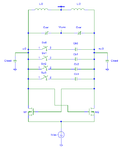
In order to understand this case in more detail. I have attached the schematic at the end and the main parameters are described as follows:
My target Frequency is 5GHz. L = 1.33nH. The total C vary from 30pF +/- 600fF depending on the introduction of different paths which has parallel connection with Capacitance. The MOSFETs as switch work at this part and thus the D and S ends are connected one at the Vout_negative and the other is connected with the capacitance (or the capacitor device). After passing through the capacitor the Vout_positive is connected to. Several path can be introduced in parallel. The total voltage is supplied by a Vpulse, 0V @ 0ns, 1.2V after 1ns. The total I_bias is 2.2mA.

I have noticed that the AC current drop on the ideal switch is almost 0, but on the MOSFET device, Vds_AC drops a lot. This makes fewer AC voltage drop on desired capacitance I wanted to introduce on a specific path. The AC voltage between the Vout_N and Vout_P is around 3V to 550mV in the ideal case for the 5G desired target frequency. But in the MOSFET_switch case, if this voltage is applied into the path (one MOSFET (under 1.2 V supply or bias) + one capacitor), the MOSEFT cannot only working in a stable region.

This probably the biggest problem not appearing in the low frequency domain or small signal application.
Therefore I would think of somebody shed light on how to use MOSFET as a switch in the large signal case providing not over supplying 1.2V for 90nm technology.
Or any direction on which knowledge is suitable for desiring such a large signal MOSFET switch which is also Resistance and Capacitance sensitive one?

Switch capacitor might be a good topic but I do not think the circuit need extra knowledge on how to clock it.

Attached is the circuit schematic.
VCO.png
 
Last edited:

At first sight, singled ended MOSFET switches to ground seem to be a much more convenient solution. Allocating them at both sides of the differential oscillator gives still overall balance.
 
Agreed, use common source NFETs on each drain.

Also when doing transient simulations, you should make sure that the oscillation has little distortion and the FETs are kept in saturation. Try to maximize the Q of the circuit, then decrease gm so that the loop gain is not too high.
 
At first sight, singled ended MOSFET switches to ground seem to be a much more convenient solution. Allocating them at both sides of the differential oscillator gives still overall balance.

Not sure If I am getting it.
Did you mean connect the -v/2 node to Sw0 and Cb0 and directly to ground. And +V/2 node to Sw1 and further Cb1 to ground as well. Through two path on each side instead of four paths in between?

Please make it clear if I am wrong getting it.

Thanks,
Alex
 

Status
Not open for further replies.

Part and Inventory Search

Welcome to EDABoard.com

Sponsor

Back
Top