Continue to Site

Welcome to EDAboard.com

Welcome to our site! EDAboard.com is an international Electronics Discussion Forum focused on EDA software, circuits, schematics, books, theory, papers, asic, pld, 8051, DSP, Network, RF, Analog Design, PCB, Service Manuals... and a whole lot more! To participate you need to register. Registration is free. Click here to register now.

How to turn of P channel mosfet

Status
Not open for further replies.

Dinuwilson

Advanced Member level 4
Full Member level 1
Joined
Aug 20, 2011
Messages
100
Helped
1
Reputation
2
Reaction score
1
Trophy points
1,298
Visit site
Activity points
1,985
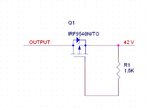
56.JPGi am using IRF9540 p channel mosfet for my solar charger.when i connect gate to groung mosfet is on. my problem is i can't turn off the mosfet


my input voltage is 42v. in this case if i connect 42 v in mosfet it alway's on . i can't connect gate directly through mosfet input (through resistor) because IRFz9540 gate voltage is +20v. in this case how i can control mosfet.
 

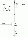
if you want to turn off the MOSFET you can use a zener diode to protect the gate, for example a 12V zener or 15V
 
thank's for your replay. where i connect the zener diode.across VIN and gate. can you post the circuit
 

i have one doubt on you circuit. if we connect like this, transistor is in off condition vin and gate voltage are same, so in this case zener diode is forward bias, so how it protect the mosfet.?
 

In the off condition, vin=vgate, so by definition the zener has no bias on it. The zener will never be forward biased.
 
In off condition vin=vgate. but ,if my input voltage is 42v then vgate=42v . maximum vgate voltage in data sheet is 20v only.
 

the role of zener is to protect the gate, so the voltage across zener will be about 15V ( if you choose a 15V zener), so you will never have 42 V in the gate
 

maximum vgate voltage in data sheet is 20v only.
To be exact, you should write Vgs instead of the meaningless term "vgate". Vgs is the difference between gate and source voltage, and is clearly limited by the zener diode.

The statement in the initial post is also wrong. In the shown circuit, the transistor is permanently off, not on.
 
  • Like
Reactions: tpetar

    tpetar

    Points: 2
    Helpful Answer Positive Rating
edaboard.JPG
Hi,

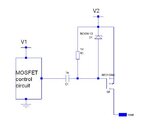
Can u try in this way.
If u have any quries on selecting components, post ur qns.

Regards,
Jebas.
 

View attachment 91590
Hi,

Can u try in this way.
If u have any quries on selecting components, post ur qns.

Regards,
Jebas.
Jebaspaul, i thing that there is something wrong on your circuit, you have to remove the capacitor, because capacitor in DC analysis will be seen us a hight impedance
 

Hi,

Please confirm one thing. What is the switching frequency of the MOSFET or the pulse width.
Capacitance value depends on the switching frequency or pulse width.

yassin.kraouch, Why are u doing DC analysis here. It is a switching circuit. the capacitance is called as "De-Coupling capacitance".

Thanks,
Jebas
 

yassin.kraouch, Why are u doing DC analysis here. It is a switching circuit. the capacitance is called as "De-Coupling capacitance".

Thanks,
Jebas

You cannot put the capacitor there since if you output a square wave from you control circuit the square wave can be seen as DC except for the transients from Low to High or High to low. By adding that capacitor you can never ground the gate of the Mosfet since the capacitor will remain constantly charged. (There is will be a boostrap thing going on but there is no need to get into it). The best way is to instead of that capacitor add a transistor with its Emitter connected to ground while the collector is connected to the gate. The control circuit is connected to the base of the transistor. This way you will have:

Control Circuit High - Transistor ON - P-channel Mosfet ON
Control Circuit Low - Transistor OFF - P-channel Mosfet OFF (Gate voltage is equal to Vsupply - Voltage drop of zener)

The circuit suggested by yassin.kraouch should be fine altough I don't thing there is the need for the 5K resistor at the emitter. That resistor will cause the voltage at the gate not to go down to 0V.
 

Hi jmsattard,

The circuit which I shared will be useful if the gate control circuitary is switching at some frequency(e:g 100 Khz).

Regards,
Jebas.
 

here is an example on how to protect the gate from higher voltage using a zenerView attachment 91551

Just simulated and it worked pretty well. Altough don't know exactly what happens. The problem I am getting is that the voltage drop due to the zener when the transistor is on is not always a constant 20V. And it seems that the voltage difference depends a lot on the 12K resistor. The bigger the resistor the bigger the voltage drop while the smaller the resistor the smaller the voltage drop.
 

Status
Not open for further replies.

Similar threads

Part and Inventory Search

Welcome to EDABoard.com

Sponsor

Back
Top