will_fung
Junior Member level 1
Hi,
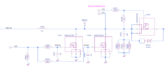
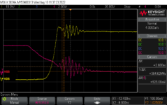
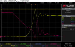
I have an issue with the BOOST circuit. with the MOSFET of NVMFS5C670NL, there is no ring on the VDS (Low side MOSFET T53201 and T53202)). But when I change to NVMFS5C646NLAFT1G, the ring on VDS is observed. I also could observe the ring on Vgs.
Could you let me know why it happened? How to solve it?
Thank you.
NVMFS5C670NL datasheet:
NVMFS5C646NLAFT1G datasheet: