vishweshgm
Member level 4
I am designing a simple buck converter to drive 9 V, 3 A LED. Supply can vary between 20 and 30 V. I used the TI Power Designer Tool to calculate the inductance value and other parameters. Here is the schematic:


After driving the load, everything is fine except that the inductor is getting heated to almost 85°C.
My PCB has to go into an enclosed box so this is not OK.
Strange thing is, the MOSFET is not getting hot at all, so the gate driving is fine, I guess. I have no clue why only the inductor gets heated in a buck converter.
Please suggest what factors concerning the inductor I should look into.
Vin : 20-30V switching frequency : 350kHz , Note that I am driving exactly 3A load (using shunt resistor (0.1ohm,2W) sensing to limit current)
Inductor HCM1A1307V2-330-R : Datasheet
Mosfet SI_4288DY : Datsheet
Diode SS54 : Datasheet
Driver IR2110 : Datasheet
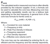
Here is the calculation screenshot of TI tool:

After driving the load, everything is fine except that the inductor is getting heated to almost 85°C.
My PCB has to go into an enclosed box so this is not OK.
Strange thing is, the MOSFET is not getting hot at all, so the gate driving is fine, I guess. I have no clue why only the inductor gets heated in a buck converter.
Please suggest what factors concerning the inductor I should look into.
Vin : 20-30V switching frequency : 350kHz , Note that I am driving exactly 3A load (using shunt resistor (0.1ohm,2W) sensing to limit current)
Inductor HCM1A1307V2-330-R : Datasheet
Mosfet SI_4288DY : Datsheet
Diode SS54 : Datasheet
Driver IR2110 : Datasheet
Here is the calculation screenshot of TI tool:
") I looked up parts, but didn't find good SMD diodes for 5A rating that I could use. Synchronous rectifier will need more space which I cannot accomodate.
I looked up parts, but didn't find good SMD diodes for 5A rating that I could use. Synchronous rectifier will need more space which I cannot accomodate.