cfreng2
Junior Member level 3
Hello all! Does anyone know how to plot the gain of a CMOS inverter? How can we get the gain of a CMOS inverter? And how can we plot it in winspice?... Please help me.
Follow along with the video below to see how to install our site as a web app on your home screen.
Note: This feature may not be available in some browsers.
I am not familiar with WINSPICE, however, in general there are two alternatives - depending on your desire.
1.) DC gain: Perform a dc-sweep and plot Vout vs. Vin. The slope of the transfer curve gives you the dc gain for each bias point of this function.
2.) AC gain: If you are interested in the frequency response, choose a suitable bias point and perform an ac analysis. The you can plot Vout(rms) vs. Vin(rms) which gives you the absolute gain as a function of frequency.
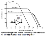
RCA posted the AC gain and bandwidth for Cmos inverters about 36 years ago. It is affected by the supply voltage. It is here:
Hello LvW,
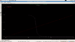
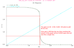
I want to use Cadence to simulate the DC gain and gain bandwidth of a CMOS inverter. I saw your post here and thank you for your information. I did the simulation for DC gain in Cadence and plotted Vout vs. Vin. But I could not be able to tell the slope of the curve. Could you please help me to do this? In the simulation, the supply voltage is 3V. I swept the Vin from 0V to 3V and got the output. I attach the plot here. Could you please have a look at it and tell me what's wrong with it? Thanks in advance.
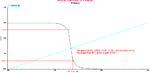
Your simulation program shows a negative image that is very hard to see. I made it into a positive image and increased the contrast.
The Sim program does not have a correct model of a Cmos logic inverter so its gain is far too low.
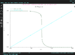
At first, increase the resolution during simulation (more points to be calculated). Your diagram shows to many "edges" and should be "smoother". Then, it should not be a problem to detrmine the slope around the linear portion of the transfer curve.
This gives you the open-loop gain.
After providing some negative feedback (as shown in the provided circuit diagram) the gain will be reduced - depending on the ratio of both transistors (as mentioned by audioguru already). This case is similar to an opamp in inverting mode.
However, the verification/calculation of the gain value depends on the (relatively large) output resistance of the CMOS stage. This is in contrast to the inverting opamp circuit.
---------- Post added at 21:39 ---------- Previous post was at 21:07 ----------
I forgot to mention that it is necessary to use an input coupling capacitor because the operating point needs dc unity gain (100% dc feedback) - in case of single supply. Otherwise the circuit cannot work as desired.
I don't think so. Ro*gm around 20 to 30 is a reasoanable number for transistors in recent standard technlogies. Applying the values from a CD4000 inverter isn't necessarily correct.The gain of the new simulation is still far too low.