Continue to Site

Welcome to EDAboard.com

Welcome to our site! EDAboard.com is an international Electronics Discussion Forum focused on EDA software, circuits, schematics, books, theory, papers, asic, pld, 8051, DSP, Network, RF, Analog Design, PCB, Service Manuals... and a whole lot more! To participate you need to register. Registration is free. Click here to register now.

How to increase thickness of wire and components using KiCAD in the SCHEMATIC

Status
Not open for further replies.

raju_kambar

Full Member level 3
Joined
Jun 19, 2013
Messages
153
Helped
5
Reputation
10
Reaction score
5
Trophy points
18
Location
Earth
Activity points
1,404
I have drawn my own desired schematic using KiCAD. I want to increase the thickness of the wires and components. How to increase the thickness of the wires and components using KiCAD software, which option I need to use. Can you suggest me.
 

Attachments

  • KiCAD_Drawn_Figure.jpg
    KiCAD_Drawn_Figure.jpg
    282.5 KB · Views: 118

I'm not sure you can, or should do that. The parts come from the library so you would have to edit all the individual component shapes to use more pixels. If you did that the schematic would look horrible!

Why do you want to do it?

Brian.
 
I'm not sure you can, or should do that. The parts come from the library so you would have to edit all the individual component shapes to use more pixels. If you did that the schematic would look horrible!

Why do you want to do it?

Brian.
Dear Sir,
Actually, If we take schematic(Which is drawn from KiCAD) as it is without making thicker. Schematic will appear as so thinner, it is not visible clearly. So I want to make it all the components such as C,R,L, power supply, voltage supply, and wire thicker, then it will be visible clearly.
For example I have shown in the below attachment file name thinner undesired. I have drawn schematic using KiCAD and print it, for this one take it as it is, crop it, wires and components are not visible clearly. So I want to make it everything thicker to visible even crop it reduce the size also.
Below I have shown two screenshots, one screen shot is desired thicker diagram(I need to draw as like desired thicker diagram), another one is undesired thinner diagram( which is drawn using KiCAD)
 

Attachments

  • Thicker_Appearnce_Desired.jpg
    Thicker_Appearnce_Desired.jpg
    36.2 KB · Views: 105
  • Thinner_Line_Appearance_Undesired.jpg
    Thinner_Line_Appearance_Undesired.jpg
    7.7 KB · Views: 128

I'm not sure if it is in all versions but on my Kicad Version: 0.201412311931+5344 if you go to:
Preferences/Schematic Editor Options/General Options
there is a box labelled "Default Line Width" which defaults to '6' but if you make the value larger it increases the connecting line and component outline widths.

Brian.
 
if you go to:preferences/Schematic Editor Options/General Options there is a box labelled "Default Line Width" which defaults to '6' but if you make the value larger it increases the connecting line and component outline widths.
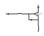
As you said, I went to Preferences/Schematic Editor Options/General Options and changed the Default bus width as 12 and saved the preferences changes. But it is not showing any increase in thickness of wires or components. It is showing as like earlier thin wire lines and components.
What I have to do, I don't know. I request you to help me.
 

Attachments

  • Preferences_KiCAD_Change.jpg
    Preferences_KiCAD_Change.jpg
    212 KB · Views: 122

I tried it under Windows version 4022 and it changes all the line widths correctly on the schematic but leaves them the same when the image is printed.

I normally use the Linux version which is currently at 5344 but I do not have access to it at the moment. If it works on later versions, you will have to compile the source code yourself or use one of the binary packages available from the Kicad web site.

As a temporary fix, you can increase the LINE width (not 'bus' as you stated but I can see you tried it anyway) then use a screen capture program. The change does not occur until you click 'OK' in the Windows version, it is immediate in the Linux version.

Brian.
 

As a temporary fix, you can increase the LINE width (not 'bus' as you stated but I can see you tried it anyway) then use a screen capture program. The change does not occur until you click 'OK' in the Windows version, it is immediate in the Linux version.
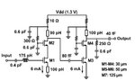
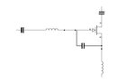
As you said I did it, now it is working nicely. But little problem I am facing, at the Gate of the Transistor Vertical line is only appearing as "thinner". Remaining everything is O.K. How to make it thicker that also near the Gate of the Transistor, which is appearing as "Thinner".

Below screen shot illustrates "thinner" appearance" at the Gate of the transistor Vertical line.
 

Attachments

  • Thicker_Appearence_Diagram.jpg
    Thicker_Appearence_Diagram.jpg
    9.7 KB · Views: 106

The line dimensions for components are held in the library. You can try this:

1. click on the component with the right mouse button to open it's properties
2. click on "Edit Component"
3. click on "Edit with Library Editor". This will open the symbol editor.
4. click on the individual lines in the symbol then click "Edit Line Options".

The box that opens will show the current line width, try changing it there.

If you want a permanent copy of the symbol with thicker lines, save it as a new component and give it a new name, maybe "MOSFET_Thick" or similar then save the library back to disc. It will then be available as a new component in the future.

Brian.
 
Status
Not open for further replies.

Part and Inventory Search

Welcome to EDABoard.com

Sponsor

Back
Top