Continue to Site

Welcome to EDAboard.com

Welcome to our site! EDAboard.com is an international Electronics Discussion Forum focused on EDA software, circuits, schematics, books, theory, papers, asic, pld, 8051, DSP, Network, RF, Analog Design, PCB, Service Manuals... and a whole lot more! To participate you need to register. Registration is free. Click here to register now.

How to feed parallel data to lots of components?

Status
Not open for further replies.

orion188

Newbie level 5
Joined
Jul 2, 2006
Messages
10
Helped
0
Reputation
0
Reaction score
0
Trophy points
1,281
Activity points
1,391
{Please let me know if this should be posted in a better group}

Hi.
I've been far from digital design for years and am not familiar with existing components and design ideas.
But as part of my current project, I have to design a system in which:

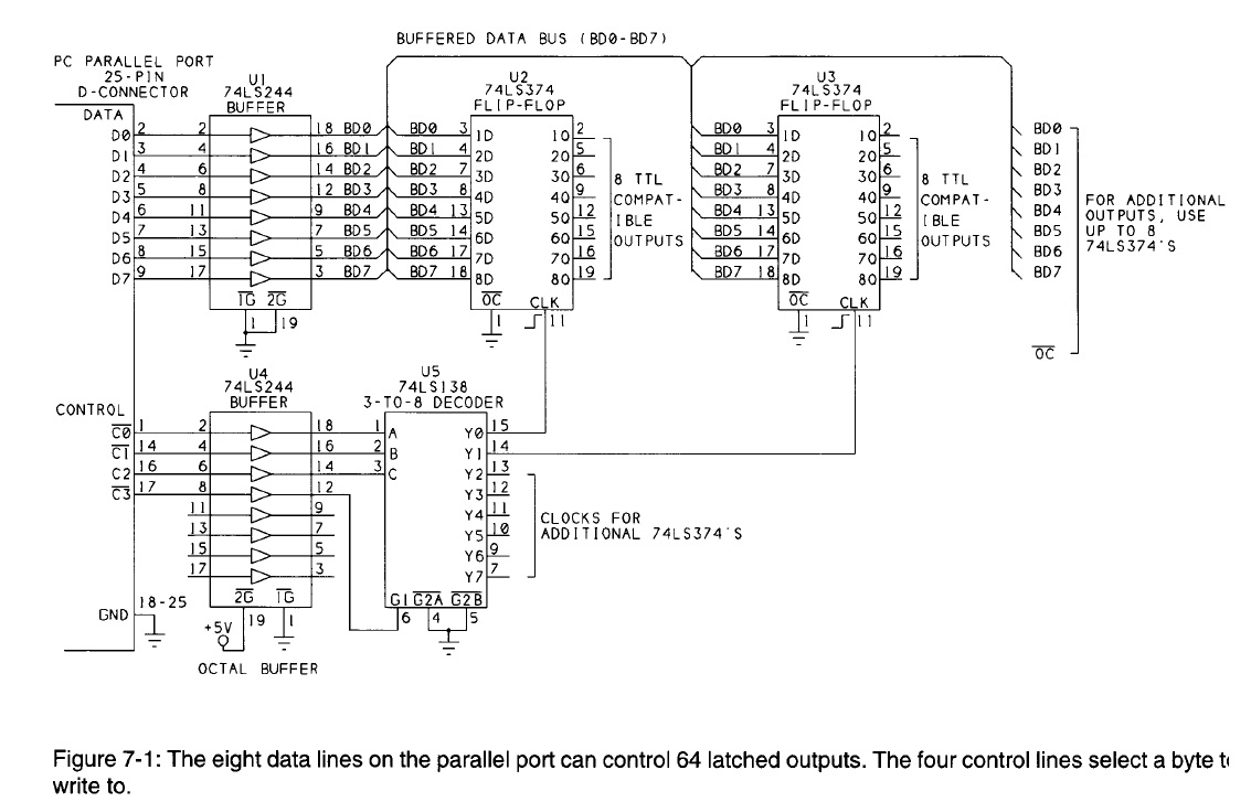
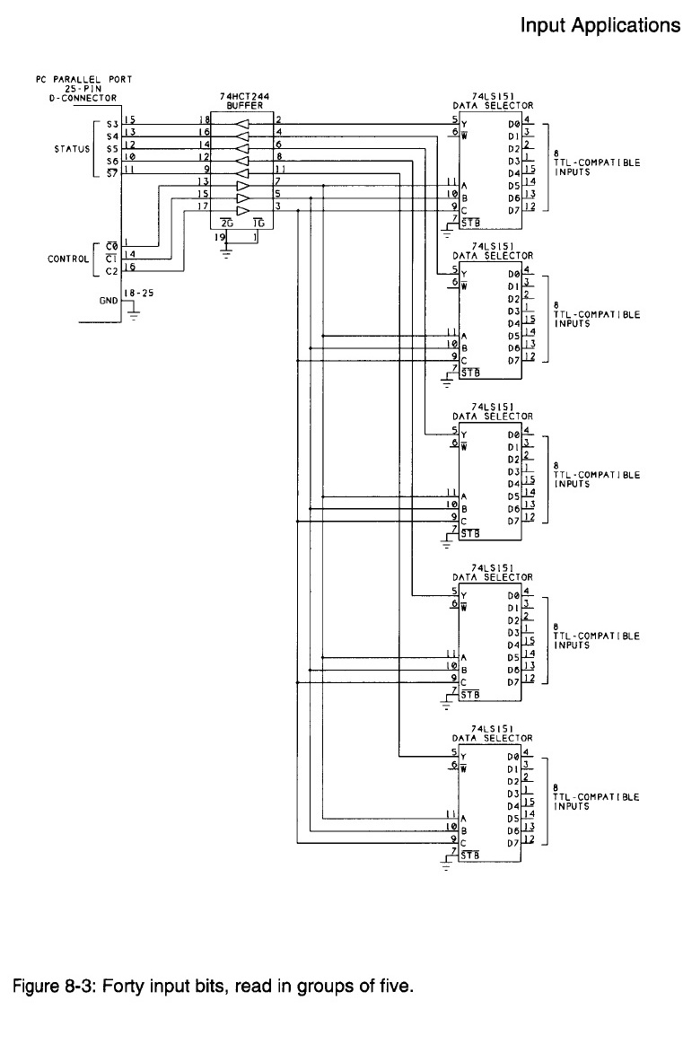
- There are 40 identical components(IC sets).
- Each component has a 14-bit parallel input.
- The system has 10 different states.
- In each state a special number should be fed to the input of each component, which is a different number for each component. (In fact we have 40 look-up tables, each having 10 rows)
- The fed data should be kept until the time comes for the next state (see? I've completely forgotten how you guys say such things in the literature )
- The system remains in each state for about 500us. So things should happen fast enough.

The very first and basic idea that came to my mind for implementing this, is to use a micro controller for, say, every 4 components. And these micro's are controlled by a master micro, or something like that!

But I'd like to know if you have any better suggestions. I think a micro controller is too bloated for just feeding a bunch of bits. How about things such as CPLDs, Shift Registers (parallel?), Memories.... something that is simple, fast and just does it's simple job? fast and clean?

I should add that the price is not currently an important factor.
Thanks in advance for your help.
 

In my view you should have a common sheared data bus and I/O expander or I/O avaliables for control signal to write the dat to sepcific device......Micro-controller will definatly help there...as your all 10 states and 40 devices can be taken care by one system.....you could have been used i2c or spi bus ....in case you have non-identical devices.....

Good Luck
 

Putting shift registers as input for all 40 ICs may be a good idea. Then control timing using 'Enable' lines of shift register may be good for your application. Then parallel all inputs of shift registers together. Now you get control to all 40 ICs.
 

@milind & gladiss
Thanks to both of you for your replies.
So I guess I should :
- At first have some kind of bus, which I don't know what it is exactly. But I guess it lets me feed the data to the devices one bye one, right?
- Then the data should be kept in the input of the devices, so you're suggesting shift registers. right? But what kind of them? SIPO? PIPO? :lol:
- I want the state changed simultaneously at the input of all the devices. How do I do that? With the Enable pin gladiss?

Thanks again guys
 

- In each state a special number should be fed to the input of each component, which is a different number for each component. (In fact we have 40 look-up tables, each having 10 rows)
- The fed data should be kept until the time comes for the next state (see? I've completely forgotten how you guys say such things in the literature )
Sounds like you could use a register (14 bits wide) for each component, that have their data inputs connected in parallel. Then you'd have 40 write strobes, with some decode logic you could reduce that to 1 write strobe + a 6 bit component 'address' select. Basically a write-only bus, consisting of 14 data bits, 6 address bits and a write strobe.

Then cycle through those addresses with some clock generate logic and say, an EPROM with the data to be written? Or a small microcontroller to do the writing to each register in turn?

Shift registers would require fewer connections but faster clocks & logic, parallel inputs would require more connections but lower-speed logic. What's easier in your case might depend a lot on what you'd use to write to it.

- The system remains in each state for about 500us. So things should happen fast enough.
That's a 500us cycle for "all outputs updated". Do you have any requirements for the time between "component 1 updated", "component 2 updated", "component 3 updated" etc. :?:
 

Thanks for your reply and sorry for the basic questions I'm going to ask :oops:

That's a 500us cycle for "all outputs updated". Do you have any requirements for the time between "component 1 updated", "component 2 updated", "component 3 updated" etc. :?:
All the components should be updated "at once".

Sounds like you could use a register (14 bits wide) for each component, that have their data inputs connected in parallel.
By 'register' one always means 'shift register', right? :???:

Question: Is there anything such as a "register bank" out there? Something that I can store, say, 64 bytes in it, and direct the bytes into the output one bye one? I think this can be achieved by cascading regular shift registers, but isn't there a compact version?
Or maybe alternatives such as EEPROMs?
 

Reason I asked about the update timing requirements is that in many cases you'd want instantaneous, but it's acceptable to have delays. For example when updating a screen you might expect old screen -> new screen, but it's okay if individual pixels are updated 1 after the other. As long as entire screen is refreshed fast / regularly enough that human eyes don't notice any flicker.

This affects the update methods you could use, and can make a lot of difference in implementation.

All the components should be updated "at once".
In that case you'd need a 2-stage process: for each component, first write new data into a temporary holding location (=register), while component uses another register to output current (previous) data. Repeat for all components (with timing delays in between), such that when done, all components still output their previous data but have the new data available locally.

Then apply a global "update" pulse that makes all components move the new data from temporary hold to output.

So technically not difficult, but you'd double the amount of registers required (and require the extra update signal). The serial vs. parallel load for writing new data would still apply.

By 'register' one always means 'shift register', right? :???:
No. Register is very generic something that can hold data. There are ones where you shift bits in serially, and there are ones where you present all bits on parallel inputs, and clock those in with 1 clock pulse. See for example 74HC574.

Question: Is there anything such as a "register bank" out there? Something that I can store, say, 64 bytes in it, and direct the bytes into the output one bye one?
Perhaps, but that wouldn't help you here as it could only output a small set of bits at a time. Read: that would re-introduce delays between updating component 1, component 2, etc.

It's fine for storing the data to be written, but if you require all outputs to update simultaneous, then at some point you need to have all data sitting ready in parallel.

It would help to know what the outputs are used for: a LED display? Do-it-yourself 'logic analyzer' ? .... :?:
 
Thank you very much for your elaborated reply.

you'd need a 2-stage process

You're right. Indeed I found something for that: 74??595. It has a storage register, so everything can be done exactly as I want it. I can load the registers serially, and with a global pulse, I can force them generate the output at once.

Question: Is there anything such as a "register bank" out there? Something that I can store, say, 64 bytes in it, and direct the bytes into the output one bye one?
Perhaps
Something such as a "register bank" can be helpful now with this new strategy. Why? Because as you remember I have 10 different states, so the data should be "loaded" to the registers every time. I don't want this 'loading' to be performed each time. What I have in mind is to have a design in which there are extra registers that kinda act as a memory. So I'd just need to do some 'shifts' and a final 'output'.
For example, let's assume I partition the components to groups each containing only 4 of them. So in each group I need:
4(components)*14(bits/component) = 56bits ==> 7 x 8-bit registers would be enough.
But to handle 10 states, I could have 10 layers, =70 registers=560 bits, all in a cascade design. Only the last layer (last 7 registers) would have their output pins disclosed. This way I can load ALL the data to the register bank, Then simply do 7*8=56 shifts and a simple 'output' at each state.

So, is there such a device out there in the market? I've searched on the net and found some 4x4 'register files'. But I need a lot more bits.

Any other suggestion is also appreciated.
And thanks again for your help man.

EDIT: It's used for an industrial system, which I don't really know what it is used for. But the specs in my contract requires my design to generate the output 'at once', and they mean in a few micro-seconds order (even if they don't really need it :wink:)
 
Last edited:

You can use SIPO shift registers such as 74164 or 74595(As others suggest). Both has enable pins. 595 is having an additional Output Enable pin also. Both work in more than 1MHz Clock. So you can definitely refresh data within 500 micro seconds. Please refer datasheet
https://www.fairchildsemi.com/ds/MM/MM74HC595.pdf
 

Do consider FAN out and FAN in capabilities of devices don't end up in sourcing or sinking more current
 
Do consider FAN out and FAN in capabilities of devices don't end up in sourcing or sinking more current

Thanks. That was a good point!
By the way, I still have an unanswered question: I need a device which is sort of a "shift register bank". Something that provides with a lot of shift registers. Something that can store, say, 64*8 bits inside.
I think I can also call this hypothetical device a "FIFO memory" or a "Sequential Access Memory". right? :?:
 

why cannt you emulate this in microcontrollers with some software coding...

Well, if I didn't mention before, because I need the output to be generated 'at once', and right after I detect some input clock.

In fact, I have come to a temporary conclusion so far: I use shift-registers with an extra layer in their output. They can respond fast enough.
The only remaining question is:
I need a device which is sort of a "shift register bank". Something that provides with a lot of shift registers. Something that can store, say, 64*8 bits inside.
I think I can also call this hypothetical device a "FIFO memory" or a "Sequential Access Memory".
 

Status
Not open for further replies.

Part and Inventory Search

Welcome to EDABoard.com

Sponsor

Back
Top