Continue to Site

Welcome to EDAboard.com

Welcome to our site! EDAboard.com is an international Electronics Discussion Forum focused on EDA software, circuits, schematics, books, theory, papers, asic, pld, 8051, DSP, Network, RF, Analog Design, PCB, Service Manuals... and a whole lot more! To participate you need to register. Registration is free. Click here to register now.

How to detect dry joint in a 900pins BGA?

Status
Not open for further replies.

klpang1

Junior Member level 2
Joined
Jan 4, 2005
Messages
20
Helped
1
Reputation
2
Reaction score
1
Trophy points
1,283
Activity points
254
Hi all,

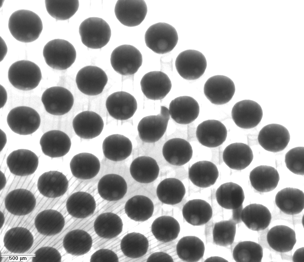
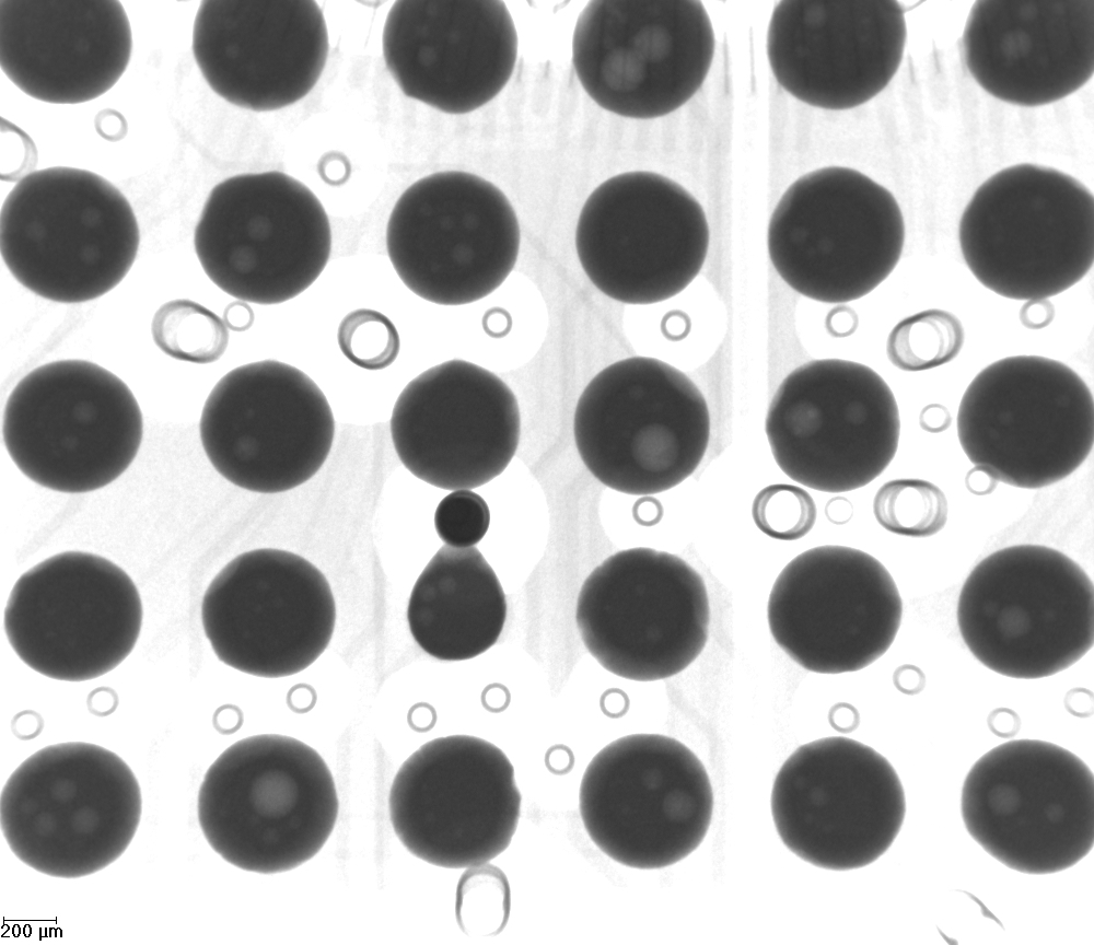
Most of our boards uses FPGA, ASICS and Processors in BGA package which may have about 900 pins each.

What is the usual method that is used to detect for dry joint on these BGA?

I am searching high and low for such a capability but to no avail. Our PCBA supplier wants nothing to do with reworking BGA as they claim that do not have such a capability. Does anyone has any ideas on the usual method to do so?

Even desoldering and reflow the component that we suspect may pose a risk as the supplier refuse to accept responsibility should the board be damage in process (pad comes off). Is BGA such a difficult thing to work with? Or are they any steps that we should adhere to in the removing and resoldering BGA's?

Any ideas? Appreciate it.

Thanks.

Best rgds,
KaKiaYam
 

There are several papers on the internet on this topic -
BGAs can be successfully desoldered/resoldered by reasonably competent assembly shops, but there is always some risk involved, dependent on the pitch and ball size of the devices, the quality of the PCB fabrication, soldermask material, aperture, pads and via sizes&locations, copper weight, etc.
Visual indpection and X-ray of the assembly can catch the more blatant/obvious ones, especially near the outer edge, but is otherwise pretty limited.
It seems a number of designers are incorporating some BIST (Built In Self Test) techniques to help address the issue/detect inferior joints (or potentially detect failed joints in the system after it has deployed). In the simpler case, it involves adding some capacitors tied to I/O pins on the device at strategic port locations and measuring the ability to charge/discharge the capacitor through external probe tips contacting various I/O test pads on the PCB, but it may not require any FPGA code additions to test in the unpowered state in production. In a more complex version, some BIST FPGA code is dedicated to check for high or low logic levels on I/O pins when a self test mode is initiated, and it may use the external, added capacitors or resistors as the test loads. I don't think that either of these cases can guarantee 100% identification rate, though, but certainly it makes sense to design in some minimal level of BIST capability as components complexity and number of connections grows higher.
 
Thanks for the reply. So you are basically saying there is no 100% way of detecting dry joint on a BGA package? What about those 2D or 3D X-Ray? Does those things equipment exist to detect dry joint, especially those in the middle of the component and not at the side? (hidden from view)


Thank you.
 

The term "dry joint" is a bit vague. You should better refer to specific failure mechanisms.

Generally, state-of-the-art X-ray will show most defective solder joints. See below an example of incorrectly masked vias that have drained solder ball metal in some cases which can be well detected on a vertical and even better on a tilted view.


Preferably, electrical connections should be checked by functional and boundary scan tests. X-ray won't be necessary for boards that passed a visual inspection and electrical test.

Presuming correctly designed boards, BGA packages are among the easy-to-solder parts.
 

Status
Not open for further replies.

Part and Inventory Search

Welcome to EDABoard.com

Sponsor

Back
Top