Continue to Site

Welcome to EDAboard.com

Welcome to our site! EDAboard.com is an international Electronics Discussion Forum focused on EDA software, circuits, schematics, books, theory, papers, asic, pld, 8051, DSP, Network, RF, Analog Design, PCB, Service Manuals... and a whole lot more! To participate you need to register. Registration is free. Click here to register now.

How to design an inverter with a MOS that has high Vds limit and low Vgs limit?

Status
Not open for further replies.

mpig09

Full Member level 4
Full Member level 4
Joined
Aug 26, 2005
Messages
232
Helped
8
Reputation
16
Reaction score
2
Trophy points
1,298
Location
Taipei
Visit site
Activity points
2,810
Hi all:

I use a high voltage tech.
The high voltage PMOS/NMOS operation condition:
a. vds : 0~40V
b. vgs : 0~5V
c. VDD is 40V

I need some logic cells to control the circuit,
do you have suggestion for design an inverter?

Thanks for your reply.
mpig
 

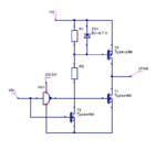
There are integrated half-bridge gate drivers for this purpose, like e.g. LM5104 from NS or L6384 from ST. If you want a discrete solution, use something like this:
HV_gate-driver.png
Use an appropriate voltage divider R1/R2 to guarantee a max. voltage drop of 5V over R1, or - if available - use the Z-Diode instead.
T3 should be a HV MOSFET, too.
 

You need to split your control signal (which had better
respect Vgs, or you have to add making a "tolerant"
input to the task) into a low-side-referred NMOS
drive chain and a high-side-referred PMOS drive
chain, and the the two come back together only
at the HV drains at the output. Since Vgs is so
limited you probably will use the "5V" devices for
the taper chains and the HV devices only in the
level shifter, the "tolerant" front end and the
final output (LV devices will be faster and have
better drive per W, when they can be used).
 

Hi erikl :

Thanks for your reply.

The solution that you post that I think it has a problem for me:
==>The chip is a LDO, and VDD of this chip is 40V. (<-sorry I didn't post it before.)
so the input signal of logic cell is 0V / 40V.
The process has 5V devices,
If add a pre-regulator for these logic cells (when use 5V devices to design),
the control signal source is still 0V / 40V.

I found Vgs < 5V for 40V MOS is difficult design for logic cell.
ex: PMOS: VDD(Vs)=40V, the vg needs > 35V.

If I have any mistake, please let me know.
mpig

- - - Updated - - -

Hi dick_freebird:

Do you mean design a Level shift to scale down the high voltage signal,
then use 5V devices to design a inverter?

If I have any mistake, please correct me.
mpig
 

Status
Not open for further replies.

Part and Inventory Search

Welcome to EDABoard.com

Sponsor

Back
Top