Continue to Site

Welcome to EDAboard.com

Welcome to our site! EDAboard.com is an international Electronics Discussion Forum focused on EDA software, circuits, schematics, books, theory, papers, asic, pld, 8051, DSP, Network, RF, Analog Design, PCB, Service Manuals... and a whole lot more! To participate you need to register. Registration is free. Click here to register now.

How to connect multiple PMOS and NMOS transistor together ?

Status
Not open for further replies.

DimaKilani

Member level 1
Member level 1
Joined
Jan 23, 2014
Messages
39
Helped
0
Reputation
0
Reaction score
0
Trophy points
1,286
Visit site
Activity points
1,648
I have multiple transistor of PMOS and NMOS and I want to connect them in a right way .. how can I do that ? for example, if I have two PMOS transistor, the drain of the the 1st transistor should be connected to the drain or source of the 2nd transistor ?

I need to know the proper way of connecting the transistor to eliminate any improper design.

Could you please answer me or provide me with useful links ?

Thanks :)
 

Why are you trying to connect them together? An H-bridge? A half-bridge? Parallel for improved current handling?
 

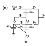
am trying to connect them in a switched capacitor circuit. I figure out that I have a gate leakage and I think that this gate leakge is due to the incorrect connection between the nmos and pmos ... Any idea ?
 

Look down the list for his earlier thread "leakage current in switched DC-DC converter" for the circuit. I only know because I was following that thread.
 

SC_1.PNG
Judging by your circuit, oh, wait a minute, I have no idea what your circuit looks like....

Here is my circuit. I just want to know the key idea of connecting both nmos transistor, pmos transistor and a combinational nmaos and pmos. No matter what the circuit is, there is a basic way that both transistor are connected in a right method.
 

View attachment 101791

Here is my circuit. I just want to know the key idea of connecting both nmos transistor, pmos transistor and a combinational nmaos and pmos. No matter what the circuit is, there is a basic way that both transistor are connected in a right method.

Wrong.

There are many ways to properly connect these devices, depending on the circuit.
 

am trying to connect them in a switched capacitor circuit. I figure out that I have a gate leakage and I think that this gate leakge is due to the incorrect connection between the nmos and pmos ... Any idea ?
Most likely an erroneous belief. A certain gate leakage of your 65 nm transistors can be expected by nature of the technology.

I agree with barry. Transistors will be connected according to the intended functionality of your circuit. If you have no clue, consult a text book or scientific papers.

I'm under the impression that you have been assigned a to an IC design project without sufficient information about the used technology or examples to learn the design methods.

Can you suggest me a book that explains how to connect transistors? Yes, am going to design an IC for switched capacitor and time passes so fast and I have not finalize my circuit because of such issues.
 

fine. what are these ways ? and how to choose the best way ?
Either PMOS or NMOS switches can be used for any of the switches you have shown. But some choices are easier than others to implement. For switches that go to ground, it is easier to use an NMOS switch, since it is easy to drive the gate of an NMOS low-side switch with a ground-referenced logic signal. Similarly, it is easier to use a PMOS switch when switching to +VBat, because it is easy to drive the gate of a PMOS switch from a logic signal that is referenced to +VBat. If the phase1/phase2 logic signal is made to range from +VBat to ground, it can serve in both of these places. But that only covers three of the eight switches in your circuit. The difficulty comes in controlling the five switches that go to neither ground nor +VBat. For such switches, neither end of the switch is ground or +VBat all the time, so the drive signal cannot be referenced to either ground or +VBat.

If you look at various designs for H-bridge switches, you will see that they sometimes use all four NMOS switches. In that case, the lower two switches are easy to switch. But the higher two switches require level-shifting gate drive. I think you would have to do something like that to control floating switches. You have to level-shift the gate control signal to any switch that is not connected to ground or +VBat. In the case of NMOS switches, you have to ensure that the gate is never negative with respect to the source. In the case of PMOS switches, you have to ensure that the gate is never positive with respect to the source.

One way to do that might be to use capacitive coupling and DC restoring in each gate drive circuit. If you really are designing an IC, and not a circuit board, I realize that you are somewhat limited as to what size capacitors you can use. But if you specify that the switching signal is always above a certain frequency, and is always 50% duty cycle, it should be possible to use small integrated capacitors in the chip. A DC restoring circuit can be made with one capacitor, one diode, and maybe one resistor. The topology will depend on the context, and I don't have a postable drawing tool handy, so I'll leave that to others to flesh out.

- - - Updated - - -

In reference to my previous suggestion for DC-restoring gate drive, I should point out a possible danger. During the start-up of the DC-restoring circuits, it is possible that some switches may be temporarily ON at the wrong time. If you turn ON enough switches (6), it is possible to cause a direct short from +VBat to ground. This may burn out the switches before the DC-restorers can settle into their proper operation.
 
Last edited:

1st question: what do you mena by the drive signal ? is it the gate drive ?
2nd question: As you mentioned: " In the case of NMOS switches, you have to ensure that the gate is never negative with respect to the source. In the case of PMOS switches, you have to ensure that the gate is never positive with respect to the source", do you mean that Vg>Vs for NMOS and Vg<Vs for PMOS ?

3rd question: when you said that the switches require level shifting gate, do you mean I have to increase the gate voltage ?
 

If you look at various designs for H-bridge switches, you will see that they sometimes use all four NMOS switches. In that case, the lower two switches are easy to switch. But the higher two switches require level-shifting gate drive. I think you would have to do something like that to control floating switches. You have to level-shift the gate control signal to any switch that is not connected to ground or +VBat. In the case of NMOS switches, you have to ensure that the gate is never negative with respect to the source. In the case of PMOS switches, you have to ensure that the gate is never positive with respect to the source.
Any reasoning why the gate voltage should not be inversed (with respect to the active gate level)?

If you review common CMOS digital or analog designs, you'll notice that the gates are usally driven by buffers swinging over the full supply range (provided all involved levels are within the voltage ratings of the respective technology). In a CMOS analog switch (respectively a transfer gate in the digital world), either the NMOS or the PMOS transistor or both of them will have an inversed gate voltage in off-state.

It should be also noted that the usual small signal MOS transistors are symmetrical and don't have dedicated source are drain terminals. In case of analog switches or transfer gates, the source and drain role can change in operation.
Perhaps I am incorrectly extrapolating from power electronics circuits with discrete MOSFETs. In those circuits the gate drive is always referenced to the source (or drain, if they are at the same potential). So maybe that kind of analysis does not apply to ICs.
 

Status
Not open for further replies.

Part and Inventory Search

Welcome to EDABoard.com

Sponsor

Back
Top