Welcome to our site! EDAboard.com is an international Electronics Discussion Forum focused on EDA software, circuits, schematics, books, theory, papers, asic, pld, 8051, DSP, Network, RF, Analog Design, PCB, Service Manuals... and a whole lot more! To participate you need to register. Registration is free. Click here to register now.
I know this is a dumb question. But, I just want to make sure what I understood was correct. TURN ON time is the time taken to charge the FET, and viceversa for TURN OFF. Can we able to calculate both by seeing a graph?
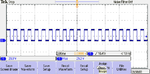
That is the picture, I got on the oscilloscope when I measured the output voltage of my circuit. I measured the output voltage at D1 from the attached date sheet by giving an input voltage of 28V, and for an inductive load. I think it makes sense for you now.
I think you want to measure the voltage at S1, not D1. When the MOSFET is off, the voltage at S1 will be 0. When the MOSFET is on, the voltage at S1 will be somewhere near Vbatt(call it Vout). Put a scope on S1 and look at the ramp that will occur when the MOSFET is turned on, then measure the time it takes to go from 0.1*Vout to 0.9*Vout. That's your rise time. You'll probably see some ringing depending on your load, wiring, etc.
This site uses cookies to help personalise content, tailor your experience and to keep you logged in if you register.
By continuing to use this site, you are consenting to our use of cookies.