Continue to Site

Welcome to EDAboard.com

Welcome to our site! EDAboard.com is an international Electronics Discussion Forum focused on EDA software, circuits, schematics, books, theory, papers, asic, pld, 8051, DSP, Network, RF, Analog Design, PCB, Service Manuals... and a whole lot more! To participate you need to register. Registration is free. Click here to register now.

how to bias BJT in large current?

Status
Not open for further replies.

prcken

Advanced Member level 1
Joined
Nov 1, 2006
Messages
419
Helped
41
Reputation
82
Reaction score
37
Trophy points
1,308
Location
Shanghai
Activity points
4,059
Hi,
I have a question about how to do bias properly for BJT in CML circuits.
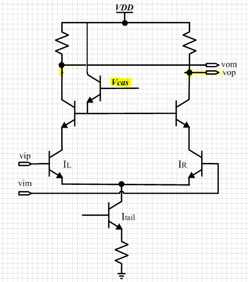
Usually in order to get a large voltage swing the current is really large (e.g. > 10mA), for high speed design, and cascoded device was added for avoiding breakdown (like the picture i attached). However, the base current for the cascoded devices (Q3 and Q4) usually won't be small, so that poses challenge for designing the Vcasc.
Basically, Vcasc drops due the base current!
I don't think just by boosting Vcasc is a good way to solve it. Do you have any comments?
Thanks!
Capture.PNG
 

If your load return is really 8V and you have that 6V rail
handy, then perhaps the 6V makes a good Vcasc. I do
not know, a priori, whether the cascode is really for voltage
division or is only to improve the Rout element of gain
(although at Zo=50 ohms, seems like you might not see
that much improvement there).

Any base impedance on those cascode NPNs is liable to
make for instability or at least degraded performance -
it will make them act quasi-inductive.

Now one question I have to ask, is why the diff pair is
not HBTs as well - why is using the MOS better in any
way, given that you are running it hot in either case?
 

I am sorry that i didn't make my statement clear. I just got a capture from a paper, and I didn't really read in detail about the distributed amplifier design. I just took an example to illustrate the Vcasc which he didn't mention in detail in the paper.
for example if I want to let Vcasc=6V, if I used a resistive divider ratio of 3/4 connect to 8V power supply, during simulation Vcasc maybe dropped to less than 5V due to the base current.
so that i really have to increase the resistor ratio to maybe 5/6.
 

Is Vcasc perhaps a control voltage, common-mode or
something? I'm guessing that is what some of the
core elaborateness is about.
 

How about a Vcasc buffer transistor?
I think that will work, but will increase the complexity of design

- - - Updated - - -

Is Vcasc perhaps a control voltage, common-mode or
something? I'm guessing that is what some of the
core elaborateness is about.
it's just a common-mode voltage which makes sure the BJT is in linear mode when the tail current is fully steered on to it.
 

To achieve large voltage swing DARLINGTON PAIR(gives high current gain) can be used.
 

you mean this?
Capture.PNG
I have to simulate and see. But I never seem people using darlington like this in high-speed design.
Thanks!
 

But I never seem people using darlington like this in high-speed design.
And it won't be a good idea due to the collector reverse transfer capacitance. Instead you would use a single emitter follower transistor as already suggested.
 

Can you please check the DARLINGTON PAIR connection.

i removed a line, still haven't got time to do simulation on it, please check the figure below
Capture.PNG

- - - Updated - - -

And it won't be a good idea due to the collector reverse transfer capacitance. Instead you would use a single emitter follower transistor as already suggested.

yes, I think the diode connected bias in the right above also will work?
 

PECL has been around for a long time driving 50Ω loads at >5GHz speeds. i don't see any advantage over tried and and true PECL buffers.

Unfortunately the purpose of the design under discussion hasn't been clearly told. As far as I understand, the cascode structure implements a high voltage supplied driver with high output level that otherwise exceeds the voltage rating of the used transistor technology. Don't compare to PECL.

To clarify what I meant with a transistor buffer:

Yes, the cascoded devices are placed there for voltage rating problem.
Do you need a current source under the emitter of the buffer?
Thanks!
 

Don't think so, why?

for this case, maybe we don't need a specific tail current for the emitter follower since it's dc voltage there, no high speed signal involved.

But for the following case, if i want to do AC coupling input a very high speed clock, e.g., 10GHz, the Vb won't be Vb1 due to the input resistance of BJT is not large like CMOS. That's another situation troubles me when biasing BJTs.
Capture.PNG
 

Vcasc is not independent and it has to be lower by at least Vce(sat) from VDD to prevent the bipolar transistor to entry into saturation.Also Vcasc defines also Vds of diff pair and Ve of bipolar pair.You should find a so proper Vcasc that satisfy those constraints.Increasing or decreasing Vcasc will not practically change the tail current but it will absolutely change the max. voltage swing.
 

Status
Not open for further replies.

Similar threads

Part and Inventory Search

Welcome to EDABoard.com

Sponsor

Back
Top