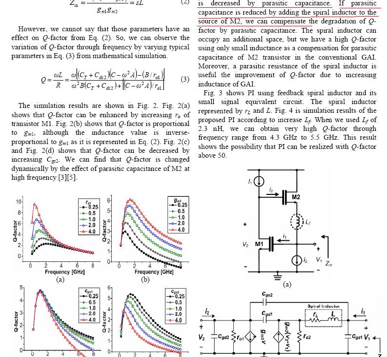
Welcome to our site! EDAboard.com is an international Electronics Discussion Forum focused on EDA software, circuits, schematics, books, theory, papers, asic, pld, 8051, DSP, Network, RF, Analog Design, PCB, Service Manuals... and a whole lot more! To participate you need to register. Registration is free. Click here to register now.
I believe what the authors are referring to is the fact that the effective inductive impedance is of opposite sign to that of the capacitive impedance. Hence, if one is considering what the total parasitic capacitance is, by adding some small amount of inductance, the net capacitive impedance appears reduced. This technique is employed to compensate for undesired lead inductance. Specifically, by adding in capacitive impedance 1/jwC = -j/wC to inductive impedance jwL, the net reactive impedance can be set to 0 at some frequency (-j/wzC + jwzL = 0).
Of course, as the frequency changes from wz, the impedance becomes non-zero for a fixed C and L. Often people use varactors for the C to allow for tuning an impedance.
I'm sure it is not obvious, but I think if you actually write the equations for the net impedance, the parallel impedance includes a net sum that does in fact reduce the net parasitic capacitance. The small signal equivalent circuit in the lower right of your image suggests there is feedback - which also suggests that the output impedance is not just the parallel combination of the inductor model and capacitor Cgs1. A numerical simulation might be an easier path to take if you have access to one.
This site uses cookies to help personalise content, tailor your experience and to keep you logged in if you register.
By continuing to use this site, you are consenting to our use of cookies.