rajan_pec
Junior Member level 2

- Joined
- Oct 22, 2007
- Messages
- 21
- Helped
- 11
- Reputation
- 22
- Reaction score
- 10
- Trophy points
- 1,283
- Location
- India
- Activity points
- 1,450
PROJECT DESCRIPTION:
There are 6 different channels or filters ( based on frequency ) to route the RF signal. Each channel or filter is made up of a circuit containing a set of PIN diodes.
To switch on to the particular channel or filter (let say channel-1)PIN diodes of that channel(ch-1)needs to be switch ON (by providing +5V) & simultaneously other channels(ch-2 to ch-6) needs to be switch OFF (by providing -75v to all respective PIN diodes).
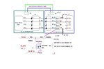
To implement this process we are considering MOSFETs as a switch, to switch ON or OFF the channels which is shown in the figure or attachment.
In the initial testing we have powered the gates of IRF6216PBF MOSFETs by using external power supplies instead of controlling through microcontroller.
Gate ,powered with 0V, results in +5.0V at the Drain pin (R33) of the respective MOSFET and gate, powered with +5V, results in -75.0V at the Drain pin (R33) of the respective MOSFET.
PROBLEM:
when using microcontroller (MCU) we are not getting same result as by using external supplies. Using a MCU, MOSFET takes more time to switch from ON to OFF state (in seconds) secondly, all MOSFETs are not behaving equally. Sometimes MOSFET switches to ON state some times it doesnot.
so we are thinking that ,some additional circuitry is required to drive the gate of MOSFET.
So plz suggest simple circuit which may help in building my project.
Regards,

Rajan
There are 6 different channels or filters ( based on frequency ) to route the RF signal. Each channel or filter is made up of a circuit containing a set of PIN diodes.
To switch on to the particular channel or filter (let say channel-1)PIN diodes of that channel(ch-1)needs to be switch ON (by providing +5V) & simultaneously other channels(ch-2 to ch-6) needs to be switch OFF (by providing -75v to all respective PIN diodes).
To implement this process we are considering MOSFETs as a switch, to switch ON or OFF the channels which is shown in the figure or attachment.
In the initial testing we have powered the gates of IRF6216PBF MOSFETs by using external power supplies instead of controlling through microcontroller.
Gate ,powered with 0V, results in +5.0V at the Drain pin (R33) of the respective MOSFET and gate, powered with +5V, results in -75.0V at the Drain pin (R33) of the respective MOSFET.
PROBLEM:
when using microcontroller (MCU) we are not getting same result as by using external supplies. Using a MCU, MOSFET takes more time to switch from ON to OFF state (in seconds) secondly, all MOSFETs are not behaving equally. Sometimes MOSFET switches to ON state some times it doesnot.
so we are thinking that ,some additional circuitry is required to drive the gate of MOSFET.
So plz suggest simple circuit which may help in building my project.
Regards,

Rajan

