Continue to Site

Welcome to EDAboard.com

Welcome to our site! EDAboard.com is an international Electronics Discussion Forum focused on EDA software, circuits, schematics, books, theory, papers, asic, pld, 8051, DSP, Network, RF, Analog Design, PCB, Service Manuals... and a whole lot more! To participate you need to register. Registration is free. Click here to register now.

high slew rate op-amp

Status
Not open for further replies.

Junus2012

Advanced Member level 5
Joined
Jan 9, 2012
Messages
1,552
Helped
47
Reputation
98
Reaction score
53
Trophy points
1,328
Location
Italy
Activity points
15,235
Hello

I found some op-amp design with slew rate in the order of several hundreds V/µV. I am just inquiring how to provide the required current for this condition if the capacitor is like 10 PF.

Thank you in advance
 

In most opamps, the slew rate is limited by the current that can be forced through Cdom by the input stage, but since most opamps use a long-tailed-pair input stage, that current is limited to double the quiescent current through the input devices.

To increase the slew rate with that kind of topology, you have to either reduce Cdom and/or increase the idling current, but there's obviously practical limits to how far you can go without running into other problems with e.g. quiescent power dissipation or input bias currents.

One neat way out of the trap is to start with an input stage whose maximum output current is much higher than it's idling current. Essentially, you need a class AB input stage.

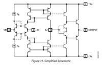
For example, the pic below shows a simplified schematic of the AD844, which boasts a slew rate of 2000V/uS. It's a little unusual in another respect as well, since it's better suited to current feedback than voltage feedback. As the datasheet explains.....


CIRCUIT DESCRIPTION OF THE AD844
A simplified schematic is shown in Figure 31. The AD844 differs from a conventional op amp in that the signal inputs have radically different impedance. The noninverting input (Pin 3) presents the usual high impedance. The voltage on this input is transferred to the inverting input (Pin 2) with a low offset voltage, ensured by the close matching of like polarity transistors operating under essentially identical bias conditions. Laser trimming nulls the residual offset voltage, down to a few tens of microvolts. The inverting input is the common emitter node of a complementary pair of grounded base stages and behaves as a current summing node. In an ideal current feedback op amp, the input resistance is zero. In the AD844, it is about 50 Ù.
A current applied to the inverting input is transferred to a complementary pair of unity-gain current mirrors that deliver the same current to an internal node (Pin 5) at which the full output voltage is generated. The unity-gain complementary voltage follower then buffers this voltage and provides the load driving power.

 
Thank you very much godfryl

this is the first time that I see you in this forum :)

is it possible to use the class AB input stage as normal as the source coupled differential amplifier op-amp ???

if you have some materials about this topic please provide it me

Also I would ask you further, what about the class AB in the output stage ?? or using an external biasing circuit to inject the current in the output capacitor at the time of slewing. I would like to discuss all of theses with you.

Thank you once again

In most opamps, the slew rate is limited by the current that can be forced through Cdom by the input stage, but since most opamps use a long-tailed-pair input stage, that current is limited to double the quiescent current through the input devices.

To increase the slew rate with that kind of topology, you have to either reduce Cdom and/or increase the idling current, but there's obviously practical limits to how far you can go without running into other problems with e.g. quiescent power dissipation or input bias currents.

One neat way out of the trap is to start with an input stage whose maximum output current is much higher than it's idling current. Essentially, you need a class AB input stage.

For example, the pic below shows a simplified schematic of the AD844, which boasts a slew rate of 2000V/uS. It's a little unusual in another respect as well, since it's better suited to current feedback than voltage feedback. As the datasheet explains.....


...... It's a little unusual in another respect as well, since it's better suited to current feedback than voltage feedback. As the datasheet explains.....

It is not only "better suited" to current feedback - it is one the best known current-feedback amplifiers (high resistive non-inverting and very low resistive inverting terminal).
 
The slew rate of classical VFB amplifiers is usually defined by compensation capacitor and the input stage current. CFB amplifiers are not limited by this parameters.

The original question is rather vague because you are not referring to OP structure details.
 
Discussion became so hot with the attendance of the analog leaders FvM and LvW :):)

guys please a little bit with me

I want for general purpose op-amp or OTA with the very high slew rate, I finished one design based on the adaptive biasing technique, this technique supposed to be good but after I finished finish my work I found it not that efficient

The only problem of, I can not imagine such slew rate in terms of hundreds µV/s... As you mentioned FvM, the slew rate is defined by the compensation capacitor. please consider if your load is 50 PF, and the compensation capacitor is 10 PF, the expected current for 100 µV/s is about 1.2*10*PF*100 µV/s= 1.3 mA

now any one tell me how we could bias the op-amp with 1.2 mA ??? I am talking about the CMOS op-amp

I jsut tried to find the answer of this , I found in Baker book page 727, a topic of source cross coupled pair, may be this will be the answer

looking for more discussion
welcome all
 

Some numbers are obviously wrong. µV/s ≠ V/µs, I a presume you are talking about the latter. V/µs translates to mA/nF.

Regarding OP structures, I must admit that I'm not in the IC design business and looking at amplifier topologies primarly from a circuit designers viewpoint. My knowledge of internal structure is fed by text books and commercial IC datasheets rather than designing them actively.

Fast OPs (in 50 MHz and above GBW class) have usually low output impedances and high output current capability (up to several 100 mA). Moderate load capacitance is not primarly affecting slew rate but possibly stability.
 

Hi Junus,

I am not quite sure what you really are asking.
Perhaps the following helps a bit:
As FvM has explained, there are opamps in current-feedback topology (CFB) which have very high slew rates.
More than that - since several years there are also VOLTAGE-feedback available (using parts of the CFB input scheme) which have similar high slew rates.
If you like to know how the work you have to go into the details of the internal structure. It`s best to start with the principle of CFB amplifiers (sometimes called transimpedance amplifier, TIA)
 

Thank you LvW and FvM

you want to say that at very large slew rate, there is a another amplifier topologies , it is different from the usual one that i am using like the folded or two stage OTA ??

my told me to design with either folded or current mirror or Two stage OTA, this why the biasing current is a problem for me. and actually i dont know about the current feedback amplifier

Thanks alot


Hi Junus,

I am not quite sure what you really are asking.
Perhaps the following helps a bit:
As FvM has explained, there are opamps in current-feedback topology (CFB) which have very high slew rates.
More than that - since several years there are also VOLTAGE-feedback available (using parts of the CFB input scheme) which have similar high slew rates.
If you like to know how the work you have to go into the details of the internal structure. It`s best to start with the principle of CFB amplifiers (sometimes called transimpedance amplifier, TIA)
 

Status
Not open for further replies.

Part and Inventory Search

Welcome to EDABoard.com

Sponsor

Back
Top