Continue to Site

Welcome to EDAboard.com

Welcome to our site! EDAboard.com is an international Electronics Discussion Forum focused on EDA software, circuits, schematics, books, theory, papers, asic, pld, 8051, DSP, Network, RF, Analog Design, PCB, Service Manuals... and a whole lot more! To participate you need to register. Registration is free. Click here to register now.

High Side MOSFET Heat Problem

Status
Not open for further replies.

fethiyeli

Full Member level 4
Joined
Feb 9, 2013
Messages
207
Helped
10
Reputation
20
Reaction score
12
Trophy points
1,298
Activity points
2,986
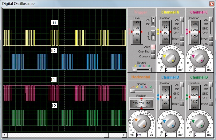
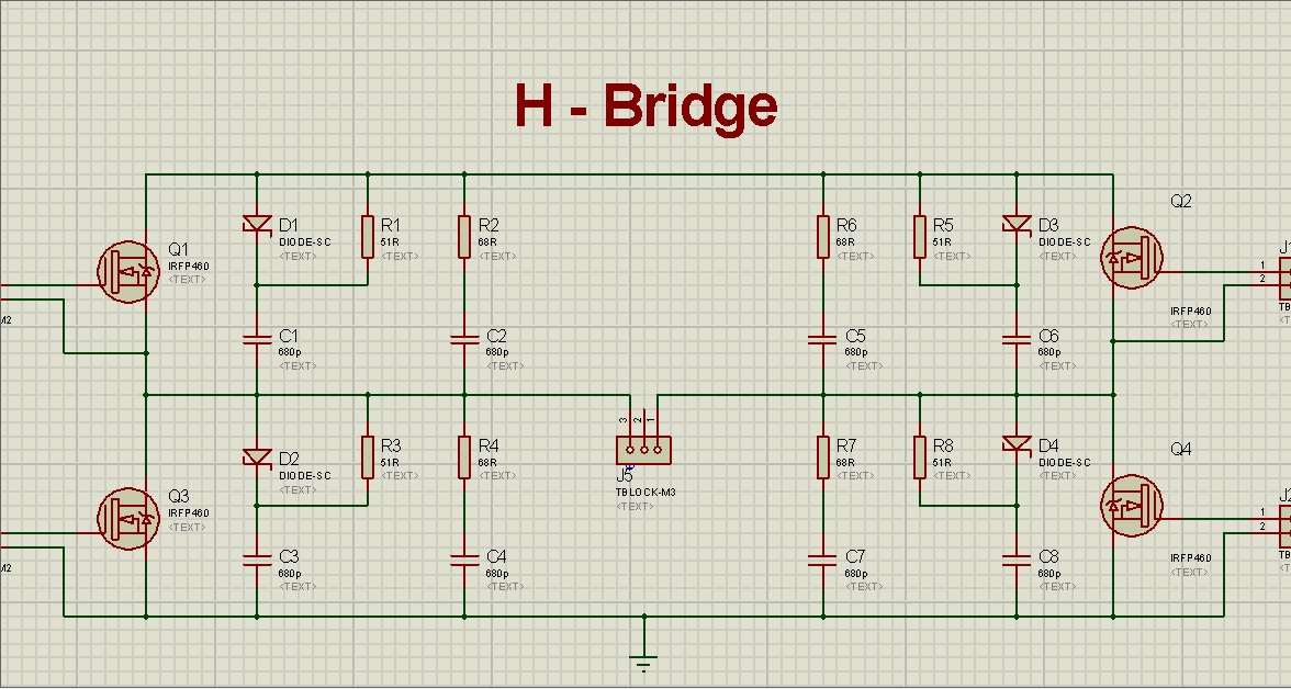
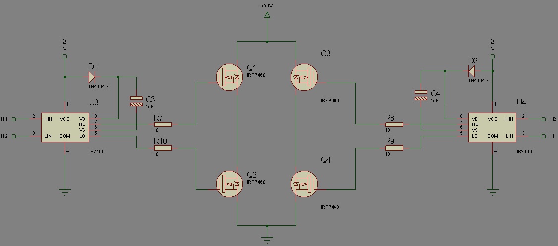
Hi everyone. I added a pic that includes 4 gate signals from TL494. L1 and L2 are output of TL494,whereas H1 and H2 inverted version of TL494 output. My problem is that when ı drive the mosfets with these 4 gate signals, high side of the mosfets become so hot. (DC Bus = 50V, it will be 311V later) I can obtain sine signal with appropriate filter. I will also ask that is this low side of the gate signals are normal ? are they supposed to be like high side of gate signals ? and can ı drive whole h-bridge with using just two H1 and H2 signals, ofc Q1-Q4, Q2-Q3 will have the same gate signals.(ignore the snubbers)

9269421500_1366132864.jpg

1380077900_1366133579.jpg
 

Serial topic at edaboard: driving a H-bridge without suitable level shifting driver for the high side.
 

Now ı understand that ı am newbie at both power electronics and edaboard =)
 

Sorry for only posting a minimalist comment. But I was guessing in part because it's not completely clear how the voltages shown in the waveforms are probed. And there's no driver schematic at all. Thus I assumed that all shown gate voltages are ground referenced.

But the high side transistors must be driven with 0/12V relative to it's source terminals.
 
Signals shown above are just the examples of my real pwm signals. I showed like that because ı obtained pwm signals almost like this oscilloscope shown above. In my previous circuit, ı have used IR2106 but now ı am using IR2110. Oscilloscope signals are ground referenced. L1 and L2 are outputs of two TL494. H1 and H2 are inverted version of L1 and L2. H1 and H2 looks like normal but others not. When ı drive mosfets with like this driver circuit, my high side of mosfets become very hot even there is no load. Notice that now ı just want to use H1 and H2 signals for both low and high side mosfets. As you see, H1 and H2 will be input of drivers. is this possible ? All the gate signals should be like H1 and H2 ?

H1 and HI1, H2 and HI2 are same.

8789495900_1366138484.jpg
 

Now ı understand that ı am newbie at both power electronics and edaboard =)
Use a high-lw driver IR2110 , and dont ever forget to add a gate to source resistor 1K
 
Signals shown above are just the examples of my real pwm signals. I showed like that because ı obtained pwm signals almost like this oscilloscope shown above. In my previous circuit, ı have used IR2106 but now ı am using IR2110. Oscilloscope signals are ground referenced. L1 and L2 are outputs of two TL494. H1 and H2 are inverted version of L1 and L2. H1 and H2 looks like normal but others not. When ı drive mosfets with like this driver circuit, my high side of mosfets become very hot even there is no load. Notice that now ı just want to use H1 and H2 signals for both low and high side mosfets. As you see, H1 and H2 will be input of drivers. is this possible ? All the gate signals should be like H1 and H2 ?

H1 and HI1, H2 and HI2 are same.
I wonder what's the purpose of the shown PWM scheme and what are L1/L2 good for? When pausing low side drivers for 10 ms, bootstrap capacitors must be quite large.

VS is incorrectly floating in your latest schematic.

and dont ever forget to add a gate to source resistor 1K
See my comment in a previous thread https://www.edaboard.com/threads/285399/#post1219991
 

I wonder what's the purpose of the shown PWM scheme and what are L1/L2 good for? When pausing low side drivers for 10 ms, bootstrap capacitors must be quite large.

VS is incorrectly floating in your latest schematic.


See my comment in a previous thread https://www.edaboard.com/threads/285399/#post1219991

hi

plz check the switch is fully ON it may operate in active region due insuffiendt gate voltage or qgd charge

check the voltage across switch(FET) when it is ON

thanks
 
L1 and L2 are for low side mosfets. As ı said ı have shown the pwm signals just for example. ı used these pwm signals for driving low side mosfets since bootstrap can charge with these low side PWM signals. So ı didnt use any isolated power for gates. In my new schematic, ı used IR2110 with gate-source resistors.

I will pay attention to your advices. Thnx.
 
Last edited:

Status
Not open for further replies.

Part and Inventory Search

Welcome to EDABoard.com

Sponsor

Back
Top