tretmax
Newbie
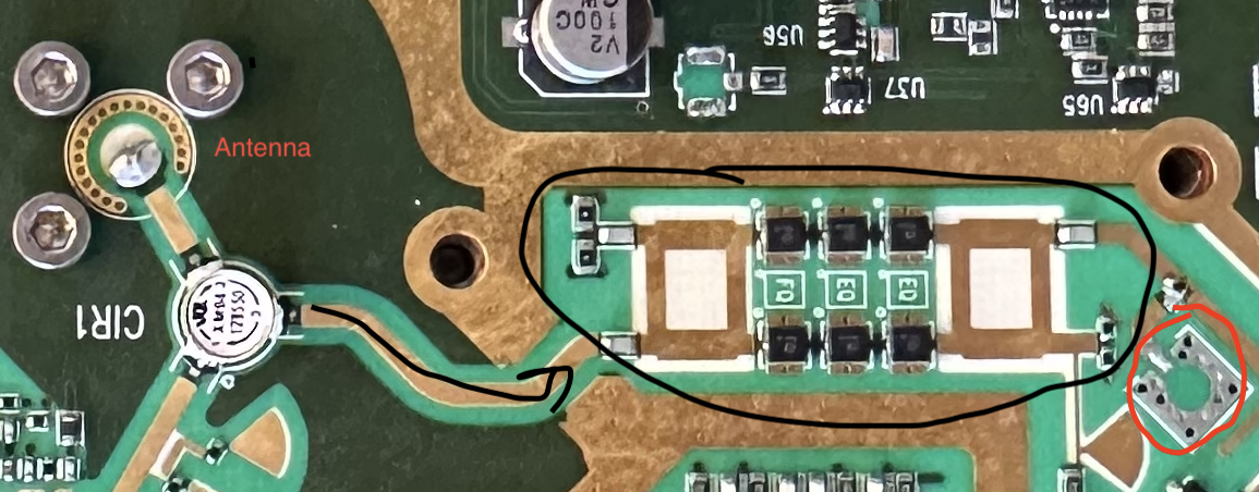
Hey, i got broken marine radar and checking if i am able to fix it, but before i need to get full picture how it works and i still not fully sure if i got correctly this part of PCB.
Context: pulse radar, working range 9.2-9.4Ghz, pretty high frequency stuff mostly looks like black magic for me.
My guess: once received signal got into antenna we shift it with 90° out of initial phase, next step cascade of 3 amplifiers for each signal(original) and (shifted 90°) and final part we combine amplified signals into 1 that shifted by 90° from original but now significantly amplified.
If it is correct, what idea of this splitting/combining for amplifying, could we get better gain like x2, also what is idea to shift original signal by 90°
Some small questions: those transistors has marking: FQ, EQ, EQ(first signal hit transistor with FQ mark) i have tried to find any of those but without luck maybe some though what it could be ?
Also not fully clear for me what is element that i circled with red, there are multiple of this kind along the micristrip lines, it is something for impedance matching ?
Thank you!