Continue to Site

Welcome to EDAboard.com

Welcome to our site! EDAboard.com is an international Electronics Discussion Forum focused on EDA software, circuits, schematics, books, theory, papers, asic, pld, 8051, DSP, Network, RF, Analog Design, PCB, Service Manuals... and a whole lot more! To participate you need to register. Registration is free. Click here to register now.

hi what could be going wrong in my schematic of Hbridge

Status
Not open for further replies.

santom

Full Member level 2
Joined
Sep 8, 2007
Messages
143
Helped
2
Reputation
4
Reaction score
2
Trophy points
1,298
Activity points
2,255
Hi all,
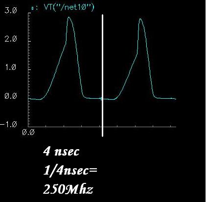
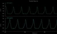
I am designing a H Bridge with suitable gate drivers.But I am getting a waveform like this.Can anyone experienced this before and if so could you please give me some good suggestions..


These signal represents to what?
Are these gate signals? and are these the result of some simulation. By looking at the waveform, I cannot understand to what they are being referred to. You H-bridge is working on which signals?
By which scheme your are powering up your h-bridge, is that PWM for square,sine wave. You need to tell about it, if you don't know.You can share your schematic, so we can understand, what kind of signals is getting into your bridge and thus producing this type of waveform.
 

Well..Thanks for the reply...I am actually doing a Power amplifier(Class D)

I have incorporated a gate driver into the H bridge circuit to drive the gates..
But I dont know whats going wrong in that..!

PLease suggest me some good guideline to go about..!
 

What type of MOSFET are these N-type/P-type or both? I cannot make the logic of gates, unless I know which are used.
Additional information about H-bridge which might be new to you, you must know about high-side and low side. High side MOSFET are more difficult to turn on as compared to low side,because the HIGH SIDE ground is floating.the lower side MOSFET turns on with ease, as the source of MOSFET is attached to ground, that's why bootstrapping is done in h-bridge. Check this up. Also I don't know if in simulation bootstrapping has anything to do. Which simulation software are you using? If you are doing simulation, so why are you incorporating the gate driver into it, you can drive the h-bridge without gate drivers?

Added after 2 minutes:

Gate drivers looks more like a steering logic to me.
 

Why is the schematic a negative with a black background covered with dots?

Why is the frequency at 1/4ns= 250MHz?

The mosfets have a high gate capacitance that the 50k resistors will take a long time to charge and discharge.
 

@audioguru
Did you calculate the frequency from the figure in this way?
41_1237839433.jpg


Added after 1 minutes:

Well.. 250 Mhz is surely a very high frequency, usually a few tens of kilohertz are used in h-bridge
 

I measured between the narrow peaks, not from the flat low part.
250MHz is 1000 times too high for a class-D audio amplifier.

EDIT:
Mosfets oscillate at that high frequency if a low value resistor is not connected in series at the gate.
 

Well..Thanks very much for your kind replies.
Now I know why I got such response graphs.
Actually it is true that we dont need any gate drivers to operate a H bridge in simulation level.

But I am undergoing a project where I should design that as it might be made in hardware level.

@umery2k75 Also what is meant by steering logic circuit.Could you explain that please.

I am using the Cadence software.
 

As you are giving only two input signal and driving 4 MOSFETS. No signal can be made that could short the power supply. It's a steering logic. Usually such circuits are provided before h-bridge, to reduce any circumstance of such logic.Such circuits are knows as steering, it's no hard and fast rule about them. You can find many circuits with the same name.

Added after 59 seconds:

Cadence PSpice?

Added after 1 minutes:

Why don't you use IC solution such as IR2110 for triggering H-bridge MOSFETS.
 

Hi
Thanks for the explanation.I am actually implementing a power amplifier in IC level.So I am trying to make my specific schematics for all of the separate sections of the power amplifier.

I just wanna know whether it is even OK to just insert some odd pair of inverters before the H bridge to do the operation.If not possible, why in some schematics they just included the inverter pairs and call that as Gate drivers.I am kinda getting confused with that.

Thanks

Santom
 

Status
Not open for further replies.

Similar threads

Part and Inventory Search

Welcome to EDABoard.com

Sponsor

Back
Top