Continue to Site
Follow along with the video below to see how to install our site as a web app on your home screen.
Note: This feature may not be available in some browsers.
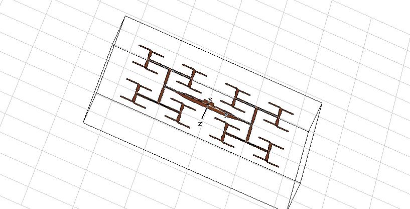
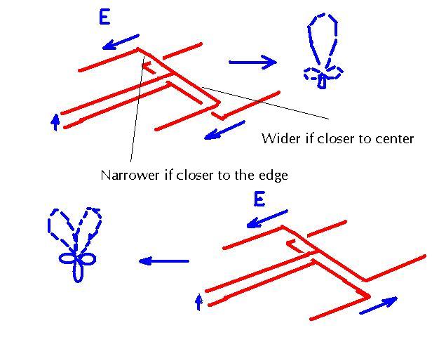
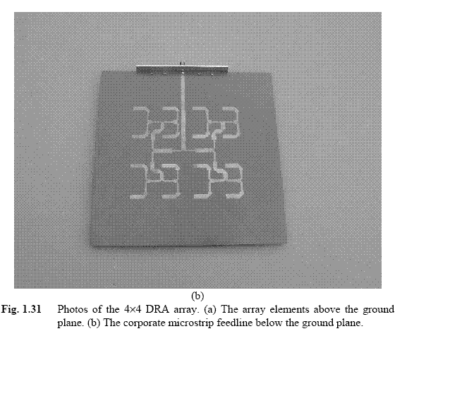
Very bad picturecostox said:Hi,
Could someone tell me what is the name of this antenna ?
Array of bended Dipole ?
THanks
oxo
") but it looks like 4 stacked dipoles.
but it looks like 4 stacked dipoles.