Continue to Site

Welcome to EDAboard.com

Welcome to our site! EDAboard.com is an international Electronics Discussion Forum focused on EDA software, circuits, schematics, books, theory, papers, asic, pld, 8051, DSP, Network, RF, Analog Design, PCB, Service Manuals... and a whole lot more! To participate you need to register. Registration is free. Click here to register now.

Help understanding diode function in bootstrapped half bridge gate driver circuit

Status
Not open for further replies.

greghagen

Newbie
Joined
Aug 23, 2022
Messages
3
Helped
0
Reputation
0
Reaction score
0
Trophy points
1
Activity points
38
I am working with a bootstrapped half bridge gate driver and I am wondering if anyone knows what function D24 is performing in the below image? I can't find this specific diode placement in any of the other circuits that I have found online. Thanks.
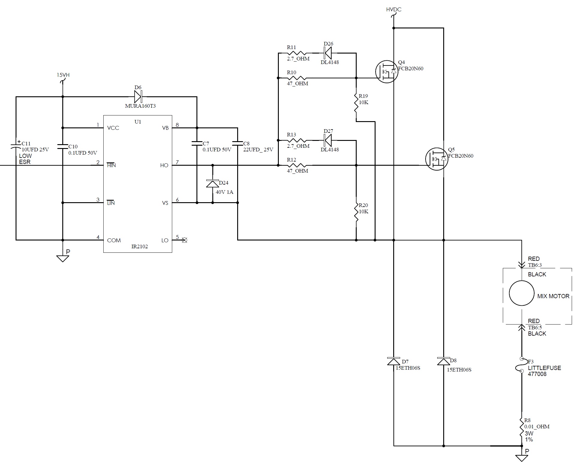
Bootstrap.jpg
 

Just a protection diode to stop HO ringing too far below Vs.
You see it recomended in the old UC3854 literature, aswell as the UC3843, but they are different chips...but they still have the said diode on the gate drive, like you show above.
 

as above - if your laoyut is poor and your re-coupling is poor on the power ckt, then IN AN HALF BRIDGE circuit the mid point can go below gnd.

In your circuit the fets are in parallel and you are using the high side part of the IC to drive these - if the bottom power diodes are any good their cathodes will only go one diode drop below gnd - assuming a tight layout.
 

Hi,

it seems you did not design the schematic on oyur own.
May I ask for the source (link) to the original schematic..

Klaus
 

That diode is standard design practice with gate drivers that use older bipolar technology, which is often the case with many pwm control chips that include an internal gate driver.
Large negative swings created by ringing may cause latchup problems or even destruction of the chip.

The application notes frequently recommend placing a fairly large Shottky diode between output and ground.

Gate driver chips these days are more likely to use mosfet technology, and of course the relatively large output mosfet inside the chip will have internal inverse diodes that very effectively clamp the output pin between ground and supply. So external diode(s) are not required.
 
Hi,
The application notes frequently recommend placing a fairly large Shottky diode between output and ground.
The diodes D7 and D8 are connected between output and GND as you say.
But OP asks about D24, which is connected between VS and HO.

I´ve never seen a diode at place of D24 in the IR2110 datasheets. (At least I can´t remember)

Klaus
 

I don't recognize a diode between HO and VS as useful measure against mid node undershoot. What should drive HO below VS? According to application note, bipolar bootstrap drivers (IRxxxx) have already an internal substrate diode between this nodes, so excursions with limited drive current will be cut without this diode.
 

it is commonly referred to in power electronic literature, when the top fet(s) turn off - if the bottom diodes don't turn on fast enough the mid point can be dragged easily 15V below gnd by the L in the output circuit
--- Updated ---

1661321871869.png
 
Last edited:

Since Klaus says there is already a "D24" inside the IR2102 i am now less sure why they use another one externally......except for the fact that its harmless so just put it in anyway.
I would have thought a UF diode from COM to VS, right at the IR2101, woudl be the best diode to use for protection.
Also, i believe Infineon owns the IR2102 now...and infineon now have some new bootstrap hi side type drivers which are a lot more immune to these switching transients than the IR2102.
 

Initially I was thinking that D24 had some kind of flyback/freewheeling characteristics to it, but what I am hearing now is that it is maybe used for MOSFET protection? The FCB20N60 has a max Vgs of +/- 30V, so I found it interesting that they went with a reverse breakdown value of 40V. I would almost think they would want a Zener for something like this or maybe something with a reverse breakdown of less than 30V.

Klaus, this is an outdated board for one of our customers that they want my company to redesign. I'm just trying to get a grasp of what D24 is actually doing before I decide if it should stay in there or not.

Thanks.
 

Hi,

Freewheeling diodes are D7 and D8. (BTW: paralleling diodes is problematic)

I can´t see how D24 can act here as useful MOSFET protection.
The best idea about it´s function maybe gave EasyPeasy: a workaround for a bad PCB layout.

One can see zeners for basic MOSFET gate protection.
(Then the diode has to be placed as close as possible to the MOSFET.)
Many Mosfets nowadays have them inside.
But combined with a IR21xx driver ... I see no use of a Mosfet protection diode at all.
(assuming a good PCB layout).

If you have the board by hand: just do a measurement whether the diode becomes conductive at all.

Klaus
 

I think there's two issues getting mixed up here.
1. Undershoot of the gate driver output below its respective reference (HO pin going negative with respect to VS, or LO going negative with respect to COM).
2. Undershoot of the half bridge's midpoint (Vs) below circuit gnd (the COM pin).
I agree with Easy Peasy that D24 is for addressing #1. True, most good drivers will either contain this diode (either because they use a MOS output, or have a separate diode in there). But there's been a couple times where I had gate drivers dying due to this, and adding such a diode was part of the solution. And those were just low side drivers for a boost converter, so #2 wasn't a factor.
 

Hi,
1. Undershoot of the gate driver output below its respective reference (HO pin going negative with respect to VS, or LO going negative with respect to COM).
LO is not connected at all thus let´s focus on HO.

Do you have a scenario or a schematic or draft how this can happen?

Klaus
 

Page 16 of this
..tells the problem.....and for the diode from Gate output to its own ground...just shovel in a SMC schottky.

Basically A bootstrap hi side driver should really have >=150v/ns of common mode immunity (CMI) to keep you safe from problems with the dv/dt of the switching node.
Your chip doesnt have this.
Digikey (and all others) unfortunately doesnt allow search on CMI though.

As discussed, infineon now have drivers which safegaurd you from all the problems spoken of in this post. With some of the infineon bootstrap drivers, the layout can be very poor, and the driver chip will still be ok.
 

Hi,

Page 16 of this
Maybe I´m dumb... I don´t see it. Not even in thedescription ... thus I refer to the schematic.

Are you talking about D1 of Figure 53?
It is connected with
* Cathode to pin 6 (bridge center via R1)
* Anode to GND.

But D24 of post#1 is connected with
* Anode to pin6 and
* Cathode to pin 7

****

Now have a look at D7 and D8 of post#1:
It is connected
* Cathode to center of bridge (without resistor)
* Anode to GND
This is almost the same as D1 of fig 53 of the datasheet, but with a current limiting resistor thus you may use a diode with lower current rating.

Klaus
 

Doesn't D24 do the same thing as the body diode on the internal NMOS? Is the assumption that the IR2102 doesn't have body diodes or maybe they just are not good enough to handle the voltage change as cupoftea was alluding to:
Basically A bootstrap hi side driver should really have >=150v/ns of common mode immunity (CMI) to keep you safe from problems with the dv/dt of the switching node.
 

{Answer to post #17}......I see what you mean, but D7 and D8 are part of the power stage...i think another diode, D1 of fig 53, is needed,, right by the chip, aswell as the D7 and D8......D7 and D8 might well not be near the bootstrap driver chip.
--- Updated ---

"gate drive design tips" by Dr Ray Ridley, actually states that Bootstrap drivers are not to be used for offline applications. Let me know if you want me to attach the doc, as i cant find it on the internet.

Here is Dr Ridleys words...

There are silicon solutions to this
problem. I would use these for low
voltage applications, but not for off-line
circuits. High-side integrated drivers
remove too much control from the
designer, and do not provide the same
level of protection, isolation, immunity
from transients, or common-mode noise
rejection as a well-designed and implemented
gate drive transformer.
--- Updated ---

Doesn't D24 do the same thing as the body diode on the internal NMOS?
yes but how do you know there is an output FET in there?.....also, a big chunky SMC schottky will have a lower vf than the internal fets body diode...so will give better protection.
 
Last edited:

As far as I see, none of the linked datasheets or application notes (in post #8 and post #16) is addressing undershoot of HO or LO node. They exclusively discuss undershoot of VS (bridge center) and measures against it.

Obviously D24 of post #1 could only protect against HO undershot. Other than claimed, I don't see a reference to possible HO undershoot in literature. If you know any, please show.

mtwieg is reporting in post #14 cases where drivers have been damaged due to gate output undershoot, although not specifically with bootstrap drivers.

Undershoot of HO can only occur if bridge center is driven up with high dV/dt by external source while HO is off, so that high side Vds is falling and Cgd driving HO in undershoot. This can hardly happen in the post #1 motor driver, but there may be circuits where it's possible. The other question is if IR21xx substrate diode can still handle the undershoot current.
 

Status
Not open for further replies.

Similar threads

Part and Inventory Search

Welcome to EDABoard.com

Sponsor

Back
Top