Continue to Site

Welcome to EDAboard.com

Welcome to our site! EDAboard.com is an international Electronics Discussion Forum focused on EDA software, circuits, schematics, books, theory, papers, asic, pld, 8051, DSP, Network, RF, Analog Design, PCB, Service Manuals... and a whole lot more! To participate you need to register. Registration is free. Click here to register now.

Help!! trying to understand this circuit

Status
Not open for further replies.

InverseUniverse

Newbie level 6
Joined
Oct 12, 2012
Messages
12
Helped
3
Reputation
6
Reaction score
3
Trophy points
1,283
Activity points
1,353
Hi All

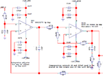
I am trying to understand what the attached circuit is trying to do but need help with that.

Looking at the circuit the first OP AMP on the left is configured as an integrator clearly as there is the capacitor in the feedback path, but I do not understand what the second op-amp is doing.

Here is my understanding of it but could be wrong: R775 / R104 are voltage dividers. R104 has current through it equal to that or R775. This stage would amplify the voltage over R104 in a positive manner.

Thanks
ques.png
 

WHat is not shown is a gain control pot for the 1k resistor in the bottom right corner to ground.

The 1st stage has ● HIGH OPEN-LOOP GAIN: 160dB
● LOW INPUT BIAS CURRENT: 10nA max
● LOW OFFSET VOLTAGE: 75µV max

The cap added tends to improve the phase margin and cuts lower than the internal cap put in all internally compensated OA's

The 2nd stage is a power amp with x10 R ratio gain

So you can see the out has 2 series 1K resistors , where the middle can be tapped to ground to attenuate the feedback which boosts the gain from unity gain up to high values. So the POwer Amp has local gain but in this design with 2 stage negative feedback the overall gain is determined by comparing the input with speaker output feedback to the 1st stage and seeing what the negative feedback resistor ratio is. So if a 100 Ohm to ground was added off the sheet, you have 10:1 reduction in feedback and thus 10:1 controlled gain with 180dB open loop gain available.

Since there is loss of phase margin with 2 stages cascaded, these power Amps also tend to oscillate at low gain high bandwidth at the unity gain resonant frequency , so the 1 Ohm load and series cap loads the spurious oscillation tendency with 1 Ohm > 50KHz to prevent it frying up with full scale RF.

Classic Audio power amp trick. So the 1st cap is not just an integrator to remove DC offset as the DC offset is removed by DC feedback loop. (1K"s in bottom right corner, so the typed info is misleading , if one did a BODE plot for phase margin , you might see the effects better.

The rest are two type of caps to minimize ESR over the frequency range on each supply rail to minimum noise, hum and shot noise. Ferrite beads might help too.
 
Last edited:

Status
Not open for further replies.

Part and Inventory Search

Welcome to EDABoard.com

Sponsor

Back
Top