Continue to Site

Welcome to EDAboard.com

Welcome to our site! EDAboard.com is an international Electronics Discussion Forum focused on EDA software, circuits, schematics, books, theory, papers, asic, pld, 8051, DSP, Network, RF, Analog Design, PCB, Service Manuals... and a whole lot more! To participate you need to register. Registration is free. Click here to register now.

Help ~~ How to simulate output impedance of a LVDS driver?

Status
Not open for further replies.

zhangljz

Member level 5
Member level 5
Joined
Oct 19, 2013
Messages
81
Helped
1
Reputation
2
Reaction score
1
Trophy points
8
Visit site
Activity points
648
Hi,

I am designing a LVDS tx, but I don't know how to simulate the output impedance. Any one can help?

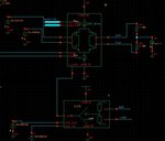
Here are my schematics.

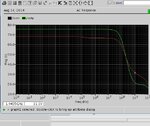
To measure the impedance,
firstly I run dc analysis to get the common-mode feedback voltage "v_cmfb". After that I disconnected CMFB circuit from the driver, and set v_cmfb to the value I got in the first step. Then connect 'outn' and 'outp' to "idc" with "dc current" 3mA, "ac magnitude 1A" "ac phase" 0 and 180 respectively. Then run ac analysi.

But the simulation shows the impedance of 'outn' is about 9k ohm, while for 'outp' only 20 ohm. Is this correct? What is wrong with the simulation configuration.

Thank you.

lvds_bias000000000000001.jpeglvds_bias000000000000002.jpeg
 

LVDS is intended to operate with a 100 ohm pin-pin impedance
attached (the transmission line and its termination). Open or
current source loaded circuits stand a good chance of sliding
to an inappropriate operating point especially when your load
current is mismatched to the internal "tail" bias current. The
pin voltages should be roughly 1.2V (or Vcm) +/- 200mV.
If they have gone much higher or lower, then you're just
characterizing an off-target condition.

Your CMFB circuit should not bother the DC solution or
transient performance (if done right). I think you should
just put 100 ohms pin-pin, reconnect CMFB, eliminate the
DC load current sources and instead inject a small current
at the pin-under-test and monitor the voltage deflection.

But because the quantity of interest is the difference voltage
and differential impedance, and CMFB would tend to take out
pin offset errors somewhat, single ended test methods may
only be good for judging normalcy at automated test, not
for validating any in-system performance.

You might therefore want to put the test stimulus across
the output pair instead, and de-embed the 100 ohm load
from the observed net Zout parallel impedance (load || driver).
 

Hello Dick,

Thanks for your reply.

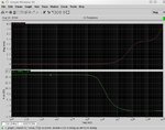
I followed your advice to reconnect CMFB, pin-pin 100 ohm resistor, and eliminate the dc current of the current source. Is the below configuration right?

However, no matter what the value of the pin-to-pin resistor, the output of 'outn' and 'outp' is the same.

Thank you.

lvds_bias000000000000003.jpeglvds_bias000000000000004.jpeg
 

If the outputs are "the same" in DC / transient solutions,
you should look to the internal operation of the driver.

The net impedance of either node ought to look like the
100 ohms.

With 70V/A showing at both pins I think the outputs are
looking like linear region, 200 ohms internal impedance or
so. That's pretty low for an output that's supposed to be
looking like a 4mA current source.
 

Both simulation setups are wrong, I fear. In the second test, you have an AC current source in series with a 100 ohm resistor. This means that the output is still operated open circuit.

What you want to do:
- terminate the LVDS driver with a 100 ohm load
- measure both differential and common mode impedance of the driver in AC analysis

For the differential measurement, it's most easy to connect a voltage source in series with the load resistor. Then measure the AC current and calculate the impedance.

For the common mode measurement, e.g. inject an AC current into a load resistor centertap.
 
  • Like
Reactions: zhangljz

    zhangljz

    Points: 2
    Helpful Answer Positive Rating
    V

    Points: 2
    Helpful Answer Positive Rating
Hello FvM,

Thank you. I am a newbee in analog design.

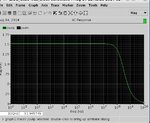
For measuring differential impedance, I connect a "vdc" source(dc voltage 0, ac magnitude 1V ) in serial with the 100ohm load resistor. In ac analysis, I got the ac current and calculated the impedance with 1/Iac. The impedance shows about 16K in low frequency.

For common mode impedance, I connect an "idc" source (dc current 0, ac magnitude 1A) in serial, and the output impedance is about 1.5K, in the case of common input voltage 0.9V.

are the both setups correct?

But for LVDS, don't we need a 50ohm output impedance to match the transmission line?
 

For common mode impedance, I connect an "idc" source (dc current 0, ac magnitude 1A) in serial, and the output impedance is about 1.5K, in the case of common input voltage 0.9V.
Where did you exactly plae the current source?

are the both setups correct?
At least the differential setup looks good, it reveals that your LVDS driver is operating as current source, which corresponds to the schematic.

But for LVDS, don't we need a 50ohm output impedance to match the transmission line?
TIA PN-4584 specifies the LVDS driver by it's differential output current. A parallel termination may be suitable at high data rates to reduce signal reflections, but isn't part of the standard.
 

The setups are shown as this:

differential impedance:
lvds_bias000000000000006.jpeg

lvds_bias000000000000007.jpeg

Common mode:

lvds_bias000000000000005.jpeg

lvds_bias000000000000008.jpeg
 

The common mode setup isn't yet right. The current source must not be connected in series with the load but between ground and output. I suggested to use a load with center tap for symmetry.
 

Hello, FvM

Thanks for your continuous concern.

Here is my setup and simulation. I think I still didn't get the point, because the impedance is so low. In dc analysis, the top and bottom transistors in LVDS are working under saturated region, so the impedance should be large.

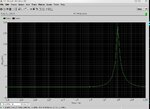
lvds_bias000000000000009.jpeglvds_bias000000000000010.jpeg
 

Setup and results look correct. The low common mode impedance is achieved by the common mode feedback amplifier, by design of the circuit.
 
Thank you, my friend.

I learned a lot from you. I will figure it out after reading some books.

Thanks again.;-);-);-)
 

Status
Not open for further replies.

Similar threads

Part and Inventory Search

Welcome to EDABoard.com

Sponsor

Back
Top