Continue to Site

Welcome to EDAboard.com

Welcome to our site! EDAboard.com is an international Electronics Discussion Forum focused on EDA software, circuits, schematics, books, theory, papers, asic, pld, 8051, DSP, Network, RF, Analog Design, PCB, Service Manuals... and a whole lot more! To participate you need to register. Registration is free. Click here to register now.

Help for understanding an Op-amp circuit ...

Status
Not open for further replies.

No22Ben

Member level 1
Joined
Sep 23, 2010
Messages
34
Helped
1
Reputation
2
Reaction score
1
Trophy points
1,288
Activity points
1,522
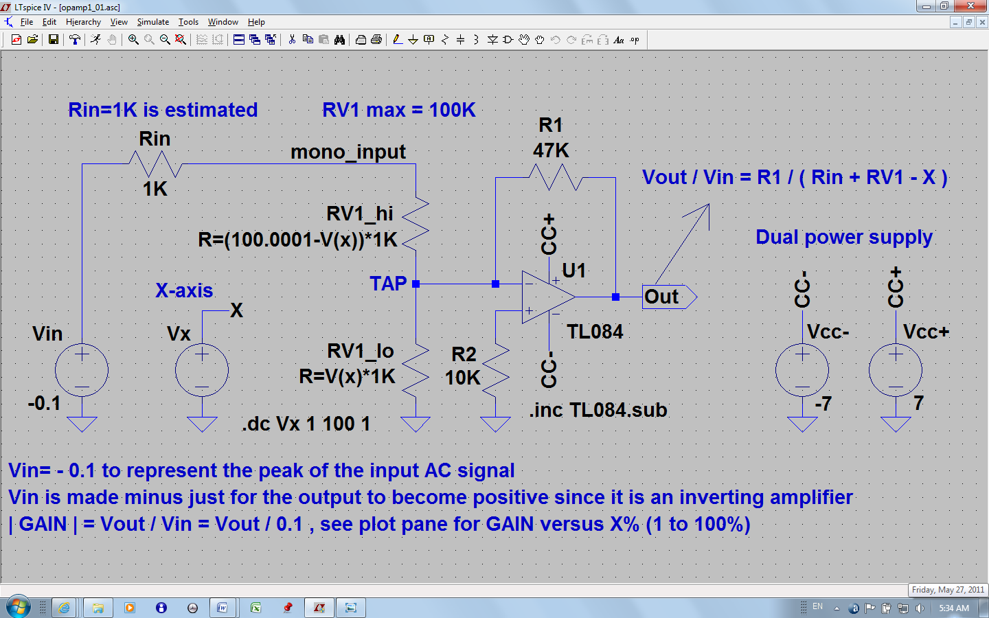
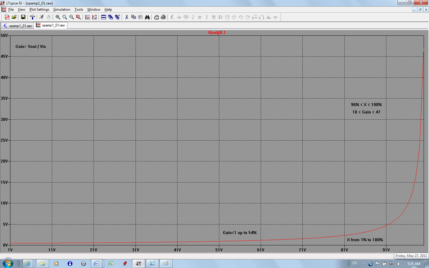
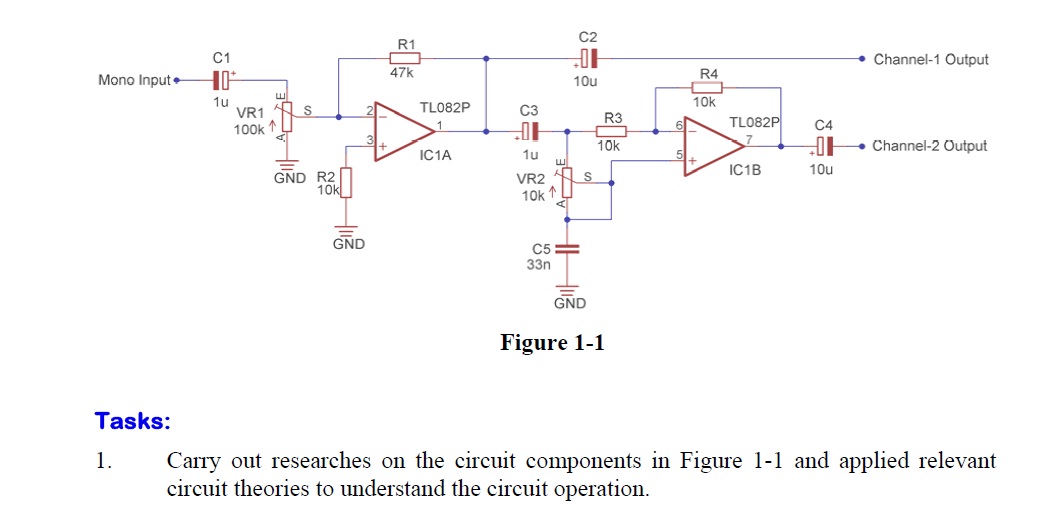
My lecturer just gave me a new assignment ... it's about operational amplifier, although he haven't teach us anything about Op-amp, but i wanna ask , what do you understand for the circuit below ??? Just want to know some suggestion, really appreciate your help ~~~ :smile:


Assignment1opamp.jpg
 

I am not sure why I can't see your circuit... hope others can help you.
 
Last edited:

Thank you for the link... now I got why I couldn't see your pic... its link happens to be a blocked one to me... sorry
 

or you can try download the image, here's the link ... **broken link removed** ... 69.24kb
sorry that I don't know which site allow us to upload photos, except blogspot >.<
 

I got it now thanks... but I agree with Alex... so I will see how we can think TOGETHER to understand this amplifier (actually a sort of preamplifier, mono to quasi-stereo).
If it is my assignment, I try to download the data sheet of its opamp TL082P first even I will be able to understand just 5% of it (Anything more than 0% is worth to work on it ;) )

Added:
Q1: Does this circuit need a power supply?

(Actually, the circuit has some wrong configurations and redundant ones, so it needs you to be prepared to understand step by step the analysis we may try to work on together... if you have time of course)
 
Last edited:
yup I think it needs power supply ...

well, my lecturer gave us 1 week to do this assignment , I haven't learn anything about Op-amp yet, so now still in researching stage ... :-?
 
Last edited:

It is good to know in advance if an opamp is supplied by a single positive source like +5V and ground (if negative, the positive terminal could be called ground) or it is supplied by a dual one like +5V, ground and -5V... which one you like to assume for this circuit? single or dual? (I know that you expect the answer had to be given by your lecturer, I think he just forgot to mention it)

Added:
For the time being, let us assume it is single as +5V, this case is rather popular. OK?
 
Last edited:

yea it looks weird for a circuit without power supply , maybe I will just mention it to my lecturer tomorrow ... thanks for your remind
 

i think this is just two op-amp with inverting mode coupled as a multistage amplifier ... first stage is an inverting amplifier... i am not sure about second stage but i think its some kind of filter.....
 
You did well.
There is a lot to talk about this circuit let us start... till you need to leave.
What is the purpose of C1 and to how far it can do its job here?
Is its polarity (as shown) right?
What may be new to you is to know the value of the resistance seen by C1 at its right side when VR1 is varied.

I assumed the circuit is supplied by 5V and ground (single supply).

Note: It is always good to get an answer after we are able to have one by ourselves first (after thinking of course) and it doesn't matter how much what we have found is right or wrong because in any case it will help us understand (and even discuss) what another may give us as an answer (supposed to be right).

Note:
If you like to go step by step in understanding this circuit (the puporse of each component, in the least), you may tell me when you can be online so I try to join you tomorrow and on the following days since you have 6 days left (now GMT is 7:35 PM)
 
Last edited:
sorry for the late reply, I had made a discussion with my coursemate today, and we seperate the circuit into 2 circuit ... here's the link , Circuit Analysis.zip ... we think that the 1st part is high-pass filter, and the 2nd part is low- pass filter ... is that correct ? and how do u think about the seperate circuit ?
 

The filter effect of the input/output capacitors is so small that is doesn't matter, it is below the audible range.
The wikipedia link I have provided in my previous post describes exactly what is the use of these capacitors.

Alex
 
sorry for the late reply, I had made a discussion with my coursemate today, and we seperate the circuit into 2 circuit ... here's the link , Circuit Analysis.zip ... we think that the 1st part is high-pass filter, and the 2nd part is low- pass filter ... is that correct ? and how do u think about the seperate circuit ?

May I give two comments?
* At first, there is certainly no single supply operation. This would not work since no bias point in the opamp linear region can be provided in this case.
* Secondly, each coupling capacitor acts as a high pass (together with the amplifier input resistor), but the 2nd stage certainly does not act as a lowpass. In contrast, the gain of this stage starts below unity and approaches unity for rising frequencies. For high frequencies, the phase goes to -180 deg.
 

sorry for the late reply, I had made a discussion with my coursemate today, and we seperate the circuit into 2 circuit ... here's the link , Circuit Analysis.zip ... we think that the 1st part is high-pass filter, and the 2nd part is low- pass filter ... is that correct ? and how do u think about the seperate circuit ?

You keep doing well, you splitted the circuit into two parts which is a good step on your part. But while I discuss with you the circuit I am afraid I have to refer to the original one and if we will have enough time, we can decide together how to make it, also step by step, a better and complete one.

As we will see, the real problem in your problem is that it is not a completely right circuit in the first place.
So some parts of it need to be discussed more in depth so that its analysis can be helpful.

Let us try clarifying some points:

(1)
The remark of 'LvW' (post #15) about the power supply is right, the first amplifier says it needs a dual supply.
The reason is that R2 is connected to ground, so as we will see, pin 3 (In+) is also at 0 voltage.
Also VR1 is connected to ground, and as we will also see the ac signal coming through C1 will try to let the opamp output be ac too (alternating between positive and negative) while ground is the reference voltage (set by R2). If the opamp is supplied by a single source as +5V and ground, the opamp1 output cannot decrease below ground. But if there is a dual supply (say +5V, 0, -5V), the output can swing into either direction. Though we can alter the circuit to accept single supply, let us assume that we have a dual one instead.

(2)
The pupose of C1 (as a coupling capacitor) is to block the DC voltage (hence DC current) from going to one stage to another in a multi-part amplifier (or alike). Therefore the polarity of C1 shows that, at its left, the input has a negative DC voltage. But if it is positive its polarity should be reversed. And in case, the input DC voltage is also zero (as the reference voltage of our opamp1), C1 should be removed. In fact, when a designer uses a dual supply for his circuit, one of his reasons might be to eliminate many coupling capacitors since almost all ac signals would have the same reference (ground or 0V).

(3)
As you said, another purpose of C1 could be to form a high pass filter. But in this case there might be two design errors. First, since C1 is a unipolar capacitor, the SIGN of its voltage shouldn't change (always positive or negative) for proper operation. Since we have no idea what are the DC and AC magnitudes of the signal at the 'mono input', we can't decide if C1 should be a unipolar or nonpolar type. Second, the input resitance seen by the C1 at VR1 side, varies with VR1 setting, from 100K to zero! (we will see why later). So it is not really a well defined high pass filter since its main RC part is not constant and also it depends on the input resistance (left of C1) which is unknown (so it could be relatively small or large).

(4)
Let us study the function of opamp1. The first thing to know about an opamp is that it has a very high voltage gain Vout/(Vp-Vn) which is too big as 1,000,000 for example (Vp=Vin+ and Vn=Vin-). Since Vout is always limited then Vp-Vn approaches zero which means Vn=Vp when the opamp is in its linear region (that is its output is between its limits, say +5V and -5V in our circuit). The second thing to know is that the input currents at Vp and Vn are relatively very small to the point they can be seen as zero in most applications (as ours). So if ask you what is the voltage at Vp (pin 3), your answer will surely be; ZERO volt, because since the input current is zero the drop on the resistor R2 is also zero. But since Vn = Vp , Vn = 0V too (how nice!). So Vn=Vp=0 is always satisfied even if an ac voltage is applied at the input.

(5)
Later, we will calculate the voltage gain of opamp1 for all settings of VR1. We will denotes by the variable x the ratio of the lower part of VR1 to 100K (its maximum range). That is 0 =< x =< 100K

See you later... if you like :wink:

Kerim
 
Last edited:
we think that the 1st part is high-pass filter, and the 2nd part is low- pass filter ... is that correct ?
The filter implemented by the second stage (without C3 in Figure 1-1) is called allpass. It has frequency independant gain of unity, and varying phase. It's discussed in the link, please notice the remark about exchanging R and C. All-pass filter - Wikipedia, the free encyclopedia
C3 shouldn't be there. I guess, KerimF has saved this problem for a future lesson, possibly next week.

You are right. And what is amazing in the circuit, is that IC1B is floating, it has no DC bias at all! I think, as you said, removing C3 is a better choice since we have already assumed that the circuit has a dual supply hence the ground is the ac reference along it.
 

Hi,

Before we continue analyzing opamp1 (IC1A) I wish to know if you already learnt Thevenin theorem since it will help easing the calculation at the input of the amplifier in order to find the formula of its voltage gain.

And to give you a quick view on how varying the tap position of VR1 affects the gain of the amplifier, I drew the circuit (IC1A) and simulated it. I uploaded both the circuit (opamp1_01_asc.png) and its plot (opamp1_01_raw.png) and both are commented.

As you will see, I had to add a resistor (Rin) to represent the internal resistance of the input source (left of mono input). I estimated its value as 1K to avoid having a zero value during the calculation (and simulation) on the denominator.

For instance, it is always important to know the resistance (actually impedance) at both the input and output of an amplifier (or alike).

Don’t forget Thevenin :wink:

See you…

Kerim


Note: Since we assumed the ac input signal has zero average voltage (that is DC voltage is zero) there is no need to keep C1. If we had to include it, I like you know that it has to be nonpolarized type in our example and its RC filter (R is the resistance sum in series with C so it equals Rin+RV1_hi only) since as we saw earlier the voltage of the tap node is always zero (grounded). So when X changes from 1% to 100%, R changes from 100K to 1K. This means if C1=1µ, the highpass cutoff frequency (1/2πRC) moves from 1.59Hz (X=1%) to 159Hz (X=100%).
 
Last edited:

KerimF: And what is amazing in the circuit, is that IC1B is floating, it has no DC bias at all

I think, that's not correct. The circuit, of course, is NOT floating. The dc bias is provided (for both input terminals) through the feeedback network.

---------- Post added at 09:50 ---------- Previous post was at 09:22 ----------

KerimF, another comment: I am not sure if your simulation arrangement (and the corresponding results) are really helpful since you have suppressed R3=10 k (see the original drawing).
 

Status
Not open for further replies.

Similar threads

Part and Inventory Search

Welcome to EDABoard.com

Sponsor

Back
Top