Continue to Site

Welcome to EDAboard.com

Welcome to our site! EDAboard.com is an international Electronics Discussion Forum focused on EDA software, circuits, schematics, books, theory, papers, asic, pld, 8051, DSP, Network, RF, Analog Design, PCB, Service Manuals... and a whole lot more! To participate you need to register. Registration is free. Click here to register now.

gm/Id methodology for designing of cs amplifier

Status
Not open for further replies.

rishabh_31ec

Member level 1
Joined
Sep 13, 2013
Messages
36
Helped
4
Reputation
8
Reaction score
4
Trophy points
1,288
Activity points
1,546
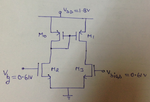
HI, I am designing the current mirror loaded single input differential amplifier using gm/Id vs. Vg and Id/w vs. Vg graph for fixed length of 360nm. I have to use bias voltage at NMOS as 0.61V and gm = 170µs. I have done all calculation by these curve considering Vds2 = 0.8V but after simulation gm and Id both are less than my requirement. What should I do?
circuit is attached in this message.......
 

Attachments

  • cs.png
    cs.png
    585.4 KB · Views: 68

... after simulation gm and Id both are less than my requirement. What should I do?
What are your desired, what your actual values? Which W/L ratios did you use? Which process?

Use current bias, not voltage bias!
 

If you are designing a differential amplifier its better not to ground the common source node of M2 & M3 .... check for conventional single ended differential amplifier architecture ...
 

Status
Not open for further replies.

Part and Inventory Search

Welcome to EDABoard.com

Sponsor

Back
Top