Continue to Site

Welcome to EDAboard.com

Welcome to our site! EDAboard.com is an international Electronics Discussion Forum focused on EDA software, circuits, schematics, books, theory, papers, asic, pld, 8051, DSP, Network, RF, Analog Design, PCB, Service Manuals... and a whole lot more! To participate you need to register. Registration is free. Click here to register now.

Generating layout from schematic in ADS 2022 without conductor

Status
Not open for further replies.

wangzhao

Newbie level 5
Joined
Sep 28, 2022
Messages
8
Helped
0
Reputation
0
Reaction score
0
Trophy points
1
Activity points
52
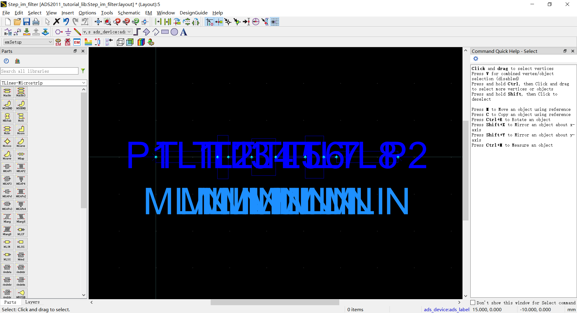
Hey bros, I drew a schematic and used [Layout] - [Generate/Update Layout] function in schematic window to create a layout.
It did create a new layout file but has no conductor(copper?), just inkprint.
Should I change substract definition or layer definition ?
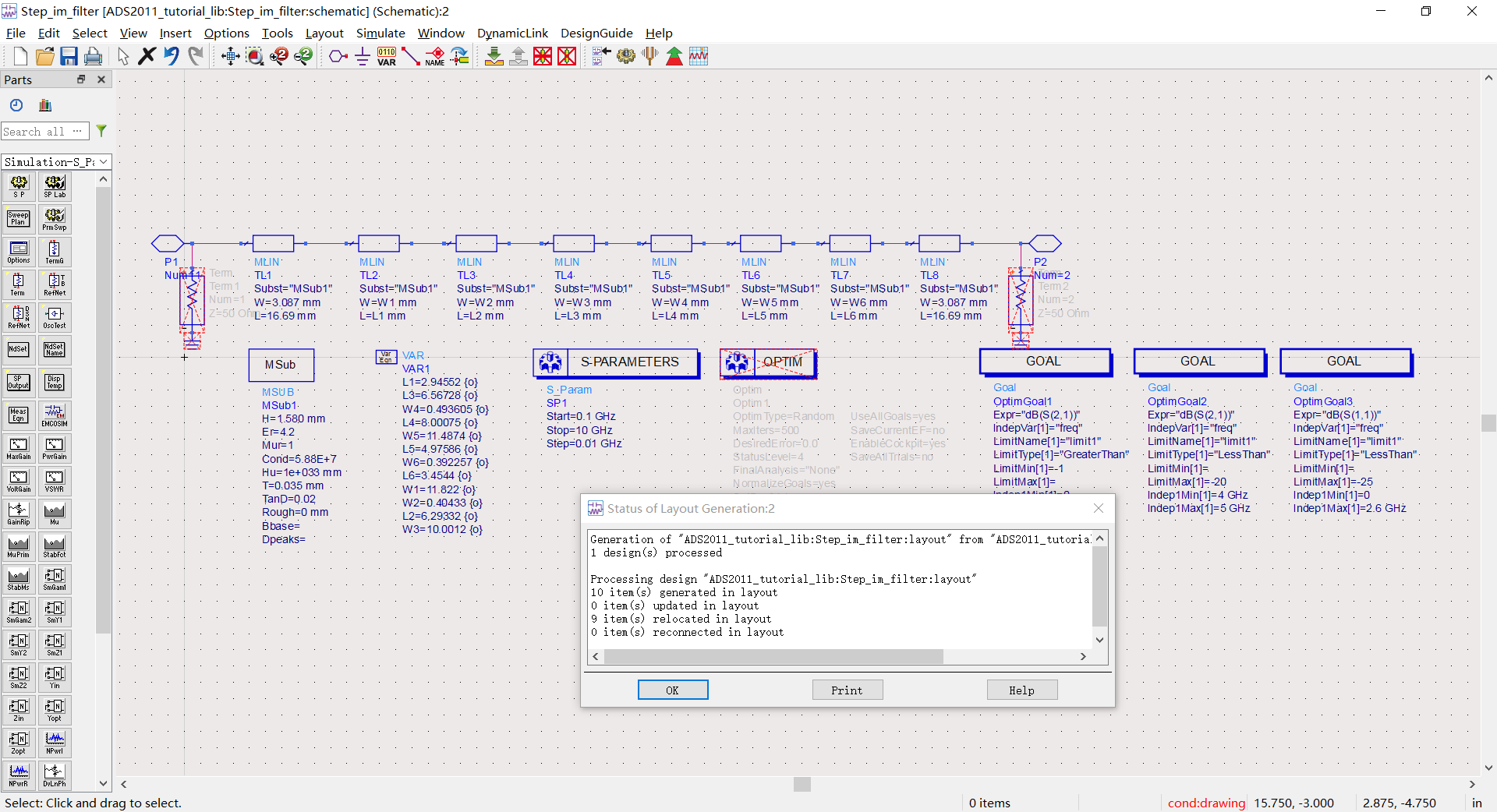
QQ截图20220928171047.png

QQ截图20220928171100.png
 

Solution
From what I see in your layout window the current entry layer is showing as ads_device:ads(_label I believe). This is a schematic layer and would only be the default if a correct layout layer technology was not applied to the workspace.

In the ADS main window select Options > Technology > Technology Setup... and you should see the following:

1664584690263.png


You are likely only seeing the ads_schematic_layers and not the ads_standard_layers. On the lower left all five of the indicators there should be green check marks. You will likely be seeing some red indications for layout layers. You should be able to reactivate this in this window by using the "Add Reference Library" button to add the ads_standard_layers library and all the check...
From what I see in your layout window the current entry layer is showing as ads_device:ads(_label I believe). This is a schematic layer and would only be the default if a correct layout layer technology was not applied to the workspace.

In the ADS main window select Options > Technology > Technology Setup... and you should see the following:

1664584690263.png


You are likely only seeing the ads_schematic_layers and not the ads_standard_layers. On the lower left all five of the indicators there should be green check marks. You will likely be seeing some red indications for layout layers. You should be able to reactivate this in this window by using the "Add Reference Library" button to add the ads_standard_layers library and all the check boxes should turn green.

Now when you regenerate the layout the transmission line should be visible.
 
Solution
Status
Not open for further replies.

Similar threads

Part and Inventory Search

Welcome to EDABoard.com

Sponsor

Back
Top