Continue to Site

Welcome to EDAboard.com

Welcome to our site! EDAboard.com is an international Electronics Discussion Forum focused on EDA software, circuits, schematics, books, theory, papers, asic, pld, 8051, DSP, Network, RF, Analog Design, PCB, Service Manuals... and a whole lot more! To participate you need to register. Registration is free. Click here to register now.

Gate Triggering Issue

Status
Not open for further replies.

sabu31

Advanced Member level 1
Joined
Jan 28, 2011
Messages
446
Helped
12
Reputation
24
Reaction score
13
Trophy points
1,298
Activity points
5,153
Dear All,

I am testing a prototype of an H-Bridge series parallel resonant inverter. When I am observing the Drain to Source Voltage.
There is some false triggering happening. after the device has turned off. What could be modified in circuit to resolve this issue.
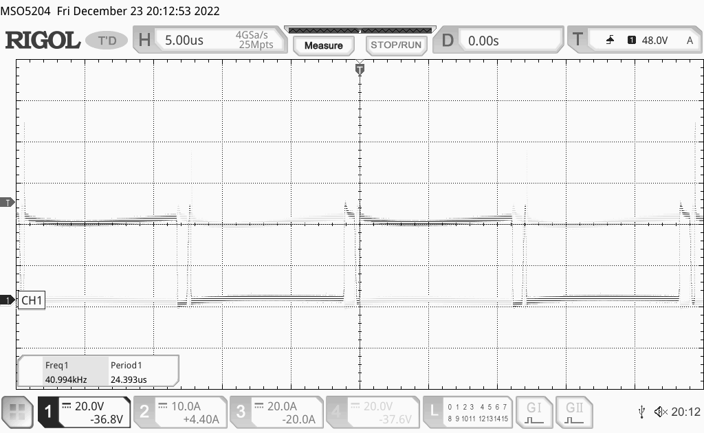
RigolDS38.png
 

Schematic ? You in a proto board or using a PCB ?

PWM have dead band timing ?

1671799728127.png


Regards, Dana.


Regards, Dana.
 

What about current sense input...it is properly filtered?
Is you gate drive too weak to bully the fet to be on or off?
Have a diode turn off in the gate of the fets......but make them turn ON slowly...see if that stops it.
 

I don't recognize "false triggering" at first sight. Please explain which voltage you are acquiring and what the expected state of high and low side transistors in the time region of interest is. I expect that in the interval between first positive edge and trigger event both transistors are off and you are seeing a kind of freewheeling oscillation. It can happen in a LLC converter if magnetizing current is too low to achieve ZVS condition.
 

    sabu31

    Points: 2
    Helpful Answer Positive Rating
You don't explain what the signals are, in the original scope capture.
It appears that your triggering is not solid. The question is why the
narrow pulse after HL. What are the 4 (?) FET gates doing meanwhile?
Is this a "commanded" rogue pulse or occurring just due to (say)
other-phase dV/dt coupling, while gates are being commanded
correctly?

You ask for the solution before doing useful debug. That is no way
to survive as a practicing engineer.
 

It's not false triggering it is your power circuit oscillating in the dead time - close up the dead time to eliminate.!
 

    sabu31

    Points: 2
    Helpful Answer Positive Rating
I don't recognize "false triggering" at first sight. Please explain which voltage you are acquiring and what the expected state of high and low side transistors in the time region of interest is. I expect that in the interval between first positive edge and trigger event both transistors are off and you are seeing a kind of freewheeling oscillation. It can happen in a LLC converter if magnetizing current is too low to achieve ZVS condition.
The voltage is drain to source voltage of the top Mosfets in H Bridge.

Is this possible in Series parallel resonant circuits during dead time?

I have kept the duty cycle at 46% and 41Khz switching.
 

It's not false triggering it is your power circuit oscillating in the dead time - close up the dead time to eliminate.!
 

For the shown operation point, reducing dead time to half the value seems appropriate. I would however prefer to see the load current waveform together with Vds. How's the waveform varying with different load amounts?
 
If this is a half bridge per phase, bootstrapped NMOSFET type power train then look at what the flying driver supply is up to. Also common mode dV/dt has a limit in those type devices, now a feature as frequencies rise and edge rates then also must.

I don't see an oscillation here, but a delay and reswitch.
 

Status
Not open for further replies.

Similar threads

Part and Inventory Search

Welcome to EDABoard.com

Sponsor

Back
Top