Continue to Site

Welcome to EDAboard.com

Welcome to our site! EDAboard.com is an international Electronics Discussion Forum focused on EDA software, circuits, schematics, books, theory, papers, asic, pld, 8051, DSP, Network, RF, Analog Design, PCB, Service Manuals... and a whole lot more! To participate you need to register. Registration is free. Click here to register now.

Gate driver output going negative

Status
Not open for further replies.

k2n2a2

Newbie level 3
Joined
Dec 29, 2012
Messages
4
Helped
0
Reputation
0
Reaction score
0
Trophy points
1,281
Activity points
1,313
Hi,

I used a gate driver from Fairchild (FAN73832) and connected it the way the datasheet shows (image 1),
and I expected that both outputs high side and low side to range from 0V to 15V.
But when I connected the chip and measured the output, the high side output ges from -5V to 10V.
I expected both outputs to switch between 0V and VCC (which is 15V in my case), did I make a wrong assumption
or is there is a mistake in the way I connected the circuit.
(I attached the oscilloscope images, which are taken between ground and pins 5 and 7 on the device)
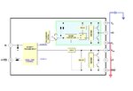
Connections.jpgFAN73832 diagram.jpgView attachment FAN73832.pdf
IMAG1410.jpg
 

From the last picture it seems that CH2 of the oscilloscope is set "AC" instead of "DC".
 

I used a gate driver from Fairchild (FAN73832) and connected it the way the datasheet shows (image 1),
View attachment 85876

Where did you see in the datasheet a wiring like the one you have applied?
Do you drive a high side and low side N mosfet like that?

The wiring I see in the datasheet is
fan73832.gif

Vs does not go to gnd but between the mosfets and Vb goes to Vcc through the bootstrap diode and there is also the bootstrap capacitor
 

I think the circuit of k2n2a2 is correct to verify the switching time. Please refer to figure 22 of the data sheet.
In any case the outputs cannot be negative. The problem is the setting of the oscilloscope: "AC" means that a series capacitor (inside to the instrument) is placed to remove the DC, then you will see a signal with zero average (i.e. having negative and positive levels).
 

You mean that the schematic he has provided was just for testing and not for the actual operation of the circuit driving the mosfets?
That is not clear from what I read in the post but in any case his connection scheme doesn't match figure 22 of the datasheet because in that there are two 15v sources, one referenced to ground and one floating so it is not the same as he did in his schematic.

fan73832-2.gif
 

Yes, I intended he was just testing the IC.
You are right, the schematic provided by k2n2a2 and that shown on the datasheet are different, at a glance they seemed to me the same. It's my mistake. However I think that with the schematic provided he should see two positive waveforms.
Of course I agree with you: to use the correctly the IC in an opertaing circuit the wiring you post in #3 have to be used.
 

Status
Not open for further replies.

Part and Inventory Search

Welcome to EDABoard.com

Sponsor

Back
Top