anushaas
Member level 5

Hi,
I am using an AD8302 IC for gain and phase measurement of two signal inputs within a frequency range of 1Hz to 1MHz.
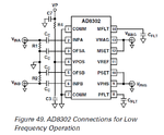
It is mentioned in the Application Note AN-691 that the IC need to be used in the following configuration to enable its use in low frequency applications.

I used a +5V supply,CC= 10uF and CFLT = 1uF.Also R1=R2 =51.9 Ohm.
The signal inputs were VINA =VF1 and VINB = VF2 as shown in the following circuit:

The voltage outputs of AD8302 corresponds to Gain and Phase measurements as per the following equations given in datasheet:

where VCP =900mV,RFISLP = 600mV/decade and RFIQ = 10mV/degree as per datasheet at low frequencies.
I acquired a bode plot for the same circuit using the Bode Analyser of NI Elvis II+ and also obtained the Gain in dB and Phase in degree using the above equations from the AD8302 output voltages.
The graphs obtained were as follows:


Can anyone please suggest ways to reduce the error in the gain and phase measurements?
I am using an AD8302 IC for gain and phase measurement of two signal inputs within a frequency range of 1Hz to 1MHz.
It is mentioned in the Application Note AN-691 that the IC need to be used in the following configuration to enable its use in low frequency applications.

I used a +5V supply,CC= 10uF and CFLT = 1uF.Also R1=R2 =51.9 Ohm.
The signal inputs were VINA =VF1 and VINB = VF2 as shown in the following circuit:

The voltage outputs of AD8302 corresponds to Gain and Phase measurements as per the following equations given in datasheet:
where VCP =900mV,RFISLP = 600mV/decade and RFIQ = 10mV/degree as per datasheet at low frequencies.
I acquired a bode plot for the same circuit using the Bode Analyser of NI Elvis II+ and also obtained the Gain in dB and Phase in degree using the above equations from the AD8302 output voltages.
The graphs obtained were as follows:
Can anyone please suggest ways to reduce the error in the gain and phase measurements?
