wandola
Junior Member level 3
Dear all, pls help me with this problem. I encountered this problem since last week. But I still don't know the reason...
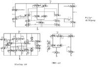
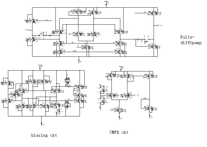
I have designed a fully-differential Opamp based on folded-cascode structure in a 60nm CMOS process. VDD = 1.2V. I choose common-mode voltage to be 600mV.
The circuit is shown below.
The Opamp AC simulation is also shown below:
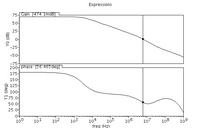
The open loop DC gain is about 70dB. GBW = 6MHz. Itotal = 97uA. PhaseMargin = 57 Degree.
Then I put the opamp in a feedback configuration to test the step response.
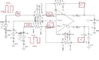
The resistor R = 200Kohms, C = 150fF.
The signals are marked in red square and waveforms are shown in Fig below.
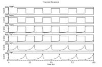
Looking at the step response simulation results, I am totally confused. What has happened to the Opamp? The inverting and noninverting inputs of the fully-diff opamp should remain at Vcm, which is 600mV. The output should be a step like response showing the settling time...
But my waveforms look weird. Can someone tell me what is wrong with my opamp?
Thanks a lot
I have designed a fully-differential Opamp based on folded-cascode structure in a 60nm CMOS process. VDD = 1.2V. I choose common-mode voltage to be 600mV.
The circuit is shown below.
The Opamp AC simulation is also shown below:
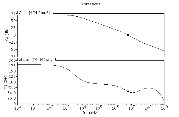
The open loop DC gain is about 70dB. GBW = 6MHz. Itotal = 97uA. PhaseMargin = 57 Degree.
Then I put the opamp in a feedback configuration to test the step response.
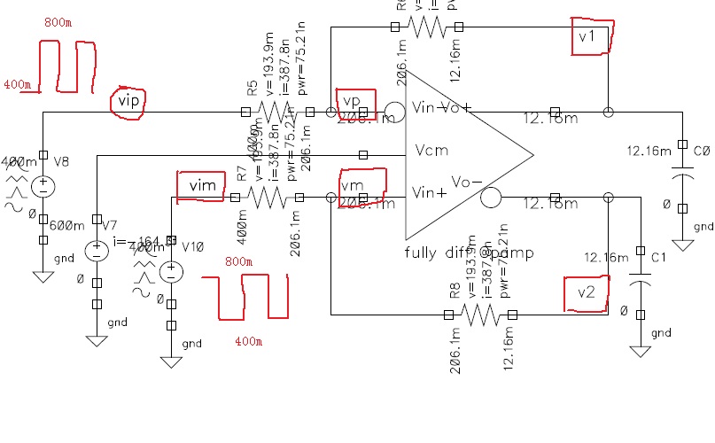
The resistor R = 200Kohms, C = 150fF.
The signals are marked in red square and waveforms are shown in Fig below.
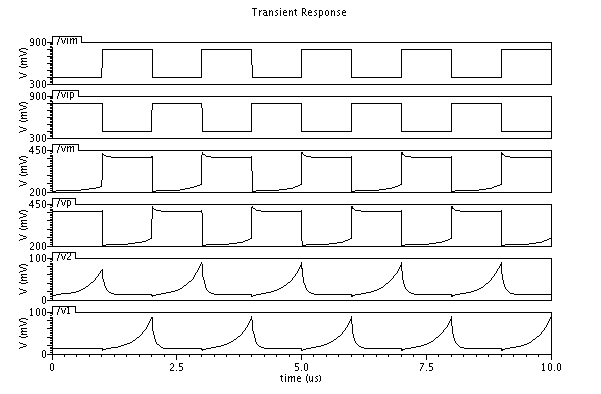
Looking at the step response simulation results, I am totally confused. What has happened to the Opamp? The inverting and noninverting inputs of the fully-diff opamp should remain at Vcm, which is 600mV. The output should be a step like response showing the settling time...
But my waveforms look weird. Can someone tell me what is wrong with my opamp?
Thanks a lot