Continue to Site

Welcome to EDAboard.com

Welcome to our site! EDAboard.com is an international Electronics Discussion Forum focused on EDA software, circuits, schematics, books, theory, papers, asic, pld, 8051, DSP, Network, RF, Analog Design, PCB, Service Manuals... and a whole lot more! To participate you need to register. Registration is free. Click here to register now.

Frequency domain FEM simulation of capacitors

dome_palp

Newbie level 4
Joined
Apr 30, 2024
Messages
6
Helped
0
Reputation
0
Reaction score
0
Trophy points
1
Activity points
59
Hello everyone,
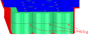
I need a suggestion about how to perform an accurate electromagnetic FEM simulation of capacitors in the frequency domain, in order to extract the impedance vs frequency curve, calculate the power losses at different frequencies in a wide frequency range (100Hz-->10MHz), map the 3D losses distribution and so detect the hotspot accurately by thermal simulation.
I made trials using Ansys Electronics tools like Q3D, but this software is not able to consider all the electromagnetic interactions correctly, in particular the displacement current.
Do you have any kind of experience in the EM model of capacitors in the frequency domain? If yes, please suggest a good general procedure to solve this kind of problems with capacitors.
Thanks in advance !
 
Don't think it's an EM problem in the first place. Exact frequency characteristic is primarily set by dielectric losses and to some amount by conductor (resistance, skin effect, inductance). For the frequency range of interest (< 10 MHz) it can be well described by lumped model parameters.
 
Don't think it's an EM problem in the first place. Exact frequency characteristic is primarily set by dielectric losses and to some amount by conductor (resistance, skin effect, inductance). For the frequency range of interest (< 10 MHz) it can be well described by lumped model parameters.
Thanks for your answer first of all !
Here below is an example of impedance and ESR measured curves vs frequency in the range 100Hz-->10MHz of 9 film capacitors connected in parallel between two busbars. As you can see, after the self-resonance frequency, there are some peaks in the ESR curve, and I'm quite sure that they are due to electromagnetic interactions in the capacitor bank (skin effect, proximity effect, and so on). I really would like to obtain the same curves by simulation, using a FEM software. Dielectric losses are present for sure, but they affect the ESR curve in the low frequencies only. Do you have any suggestion ?

1714482784015.png
 
Thanks for clarifying the focus of your analysis. You didn't talk about capacitor banks and bus bars in your first post. The bus bar can be in fact object of EM analysis, but you hardly get EM model of capacitor internals, you're stuck to lumped vendor models or your own measurement to identify the parameters.

I believe that a combination of well known capacitor impedance model (basically your impedance curve without the additional resonances above 100 kHz) and a model of the bus bar will give a good fit.
 
I fully agree to FvM: separate the problem into (a) EM analysis of the PCB routing and (b) lumped circuit model of the capcitors.

If you are interested in <10 MHz only, the routing can be considered a lumped element itself (series L + R and possibly some small shunt C), so it can analyzed at a few frequencies to extract the equivalent circuit model. The free Sonnet Lite software would be ok for analysis and circuit model extraction, but only the full product offers PCB data import. Keysight ADS would also be a very capable EM solver which offers all required functionality.

Both tools are based on MoM, method of moments. You asked about FEM - that would be overkill for this simple task, and only introduces user error if you are not experienced with the tool. The MoM tools are more user friendly and require less training to get reliable data.
Thanks for your suggestion !
Actually I tried to simulate the "physical" busbar in Ansys Q3D and the capacitors connected to the busbar modeled as series RLC equivalent circuits, but in this way I'm not able to take into account the proximity effect between the capacitors, which may be the cause of those peaks after the resonance frequency. I'm very interested in simulating those peaks and understand how to mitigate them and so obtaining lower losses. That's why I need to consider all the possible electromagnetic interactions correctly in the whole frequency range and the only way to do this is to simulate the complete physical model of the capacitor bank...
 
proximity effect between the capacitor
I'm not sure what you mean here. If you mean extra capacitance: that would be wideband, shifting resonances but not creating extra resonances.

Proximity effect is an inductive effect, and will be captured by the MoM solvers that I mentioned. However from my 25+ years work as an EM specialist: this is not relevant for your case. Skin effect and proximity effect are not causing the extra resonances that you showed.

If you have captured your layout effects already, including capacitive and inductive coupling between the lines, the extra resonances seem to be caused by a more complex behaviour of the discrete components.
You got it right.. I thought that the extra peaks in ESR and Z curves are caused by inductive effects between close capacitors in the bank at different frequencies, but you are saying that the extra peaks are actually due to something happening in the inside of capacitors themselves. In your opinion, is it possible to predict this behaviour during initial design stage, using simulation tools, before measuring the impedance of the physical component? Or is there a better way than simulation?

Thank you for your patience and support !
 
In your opinion, is it possible to predict this behaviour during initial design stage, using simulation tools, before measuring the impedance of the physical component?
I really think you need to measure the discrete components, any EM modelling would be very approximate with a lot of guesses.
 
I'm not aware of having seen multiple resonance peaks as in post #3 with single film capacitors. Thus I think it can be an effect of bus bar interconnect. Inductive coupling rather than proximity effect.
 
Thus I think it can be an effect of bus bar interconnect. Inductive coupling rather than proximity effect.
Yes, but @dome_palp mentioned that he did RLC modeling using Ansys Q3D. That tool can model mutual inductance, so I assumed that the layout model is "good enough".
 
Yes, but @dome_palp mentioned that he did RLC modeling using Ansys Q3D. That tool can model mutual inductance, so I assumed that the layout model is "good enough".
@FvM
I tried two solutions:

1) 3D model of the busbar in Ansys Q3D + equivalent circuit for each capacitor in Ansys Circuit Design, with each RLC circuit connected between pairs of Sources given by Q3D --> The simulated impedance has no peaks at all...

2) 3D model of the busbar + simplified 3D model of the capacitors in Ansys Q3D, that consists of two solid blocks with very low electric conductivity and a thin dielectric layer in between with modified dielectric constant to obtain the capacitance I want (see picture below) --> I see resonance peaks in the simulated impedance, but they don't match the measured impedance in post #3 at all...

1714647267436.png
 

Attachments

  • 1714646854867.png
    1714646854867.png
    58.5 KB · Views: 26
Last edited:
What equivalent circuit did you use for the capaciators in solution 1? Any series inductance included to model the distributed nature of the capacitor plates?
 
What equivalent circuit did you use for the capaciators in solution 1? Any series inductance included to model the distributed nature of the capacitor plates?
In solution 1 I used a very simple series RLC circuit, with the R that represents the ESR with values changing with frequency, while L and C were kept constant. All these values come from a measurement of a single film cap.
So basically, the steps of solution 1 are:
- Run a simulation of Q3D of the busbars with the solid blocks connected to the busbar, and assign Sources on the internal faces of the blocks, that represent the two terminals of each capacitor; in other words, same 3D model of solution 2, but without thin dielectric layer;
- Move from Q3D to Circuit Design and insert the equivalent circuit of each capacitor of the bank between the Sources assigned in Q3D. Divided the frequency range 100Hz --> 10MHz into 200 points and I've run a parametric circuit analysis, changing the ESR value of the equivalent circuits for each frequency.
But if I look at the overall impedance of the bank, the only resonance peak I see is the one already present in the single capacitor, but no additional resonances that appear in the real frequency scan of the bank.
It's a very difficult investigation.
 
Last edited:

LaTeX Commands Quick-Menu:

Part and Inventory Search

Welcome to EDABoard.com

Sponsor

Back
Top