Continue to Site

Welcome to EDAboard.com

Welcome to our site! EDAboard.com is an international Electronics Discussion Forum focused on EDA software, circuits, schematics, books, theory, papers, asic, pld, 8051, DSP, Network, RF, Analog Design, PCB, Service Manuals... and a whole lot more! To participate you need to register. Registration is free. Click here to register now.

Folded cascode Opamp

Status
Not open for further replies.

metuo_abeo

Newbie level 5
Joined
Feb 25, 2021
Messages
9
Helped
0
Reputation
0
Reaction score
0
Trophy points
1
Activity points
77
Hi,

I want to simulate this schematic which is a folded cascode opamp with 2 stages for a higher gain and a Miller capacitor, but I don't understand what is the role of M20 and also why the M12/13-M14/15 gates are connected together. Could someone help me to understand this schematic step by step (eg. explaining the role of each transistor)? Also, some tips for choosing W/L are welcomed or any other observations regarding this schematic.

Thanks!
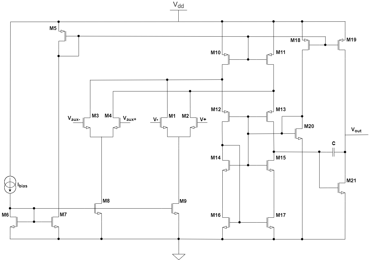
opamp.png
 

M20 is the end of a bias current repeater chain,
the current forced onto it creates a crude voltage
reference used to bias the cascode "guard" devices
M12 - M15 to roughly mid-rail. Sloppier than
providing the "guards" properly tuned N and P
biases distinct from each other. But at some Vdd
it makes sense as the guard bias points will move
toward, then past each other as Vdd reduces.
Thanks for your answer, but I didn't understand the concept of 'guard', could you describe it? Also, the bias current chain is formed of M6, M7, M5, M18, and M20?
 

The left half of the schematic is the differential amplifier (amplifiers).

(Right half)... The purpose of the current mirrors (and/or current sources) is to turn on the output stage (M19 M21) to a proper extent, so as to apply the correct voltage at the load. It does so whether it needs to sink current or source current, and it automatically calculates the amount of Amperes.
I don't know the explanation for how the network of transistors achieves this.

A general rule for an op amp's function is that the output attempts to provide a voltage to the inputs (via feedback), so that they adopt an identical voltage.
 

Status
Not open for further replies.

Similar threads

Part and Inventory Search

Welcome to EDABoard.com

Sponsor

Back
Top