Alosevskoy
Member level 3
- Joined
- Oct 11, 2011
- Messages
- 55
- Helped
- 19
- Reputation
- 38
- Reaction score
- 19
- Trophy points
- 1,288
- Location
- Zelenograd (Moscow)
- Activity points
- 1,634
Hi guys!
FIFO uses dual port BRAM to store data. The verilog description for BRAM module I wrote using the template from Xilinx's guidlines.
I've run into a problem with FIFO's simulation after P&R stage. I use Xilinx ISE.
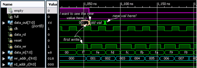
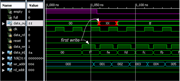
I don't understand why I get X after the first write (the FIFO was empty, i.e. write and read addresses were match) to my FIFO. For some reason the valid value ff appears only after two clock cycles (see attached pic). From BRAM Switching Characteristics table the delay from CLK to DOUT is not more then 4ns.
Someone who reads data from the FIFO monitors the empty flag, so he (or maybe she) can read out notvalid data (XX) from the FIFO (when empty goes low after the first write)... OK, I can tell someone to wait one cycle after first write before read... But maybe I'm missing something?
Any suggestions, please :smile:
Verilog descriptions of FIFO and BRAM:
FIFO uses dual port BRAM to store data. The verilog description for BRAM module I wrote using the template from Xilinx's guidlines.
I've run into a problem with FIFO's simulation after P&R stage. I use Xilinx ISE.
I don't understand why I get X after the first write (the FIFO was empty, i.e. write and read addresses were match) to my FIFO. For some reason the valid value ff appears only after two clock cycles (see attached pic). From BRAM Switching Characteristics table the delay from CLK to DOUT is not more then 4ns.
Someone who reads data from the FIFO monitors the empty flag, so he (or maybe she) can read out notvalid data (XX) from the FIFO (when empty goes low after the first write)... OK, I can tell someone to wait one cycle after first write before read... But maybe I'm missing something?
Any suggestions, please :smile:
Verilog descriptions of FIFO and BRAM:
Code:
module bram
    #(parameter ADDRW = 10, DATAW = 8)
	 (
	 input clk,
	 input we,
	 input [ADDRW-1:0] addr_a, addr_b,
	 input [DATAW-1:0] din_a,
	 output [DATAW-1:0] dout_a, dout_b
	 );

reg [DATAW-1:0] ram [2**ADDRW-1:0];
reg [ADDRW-1:0] addr_a_r, addr_b_r;

always@(posedge clk) begin
	if(we) ram[addr_a] <= din_a;

	addr_a_r <= addr_a;
	addr_b_r <= addr_b;
end
assign dout_a = ram[addr_a_r];
assign dout_b = ram[addr_b_r];


endmodule
Code:
module fifo_bram(
	clk_i,
	reset_i,
	data_wr_i,
	data_in_i,
	data_rd_i,
	data_out_o,
	status_o
    );
parameter ADDRW = 10, DATAW = 8;

input clk_i;
input reset_i;
input data_wr_i;
input [DATAW-1:0] data_in_i;
input data_rd_i;
output [DATAW-1:0] data_out_o;
output [1:0] status_o;


// addr_a <- write op
// addr_b <- read op

reg [ADDRW-1:0] wr_addr_r, wr_addr_r_nxt, succ_wr_addr;
reg [ADDRW-1:0] rd_addr_r, rd_addr_r_nxt, succ_rd_addr;

reg we;

reg empty_r, empty_r_nxt;
reg full_r, full_r_nxt;

always@(posedge clk_i, posedge reset_i)
	if(reset_i)
		begin
			empty_r   <= 1;
			full_r    <= 0;
			wr_addr_r <= 0;
			rd_addr_r <= 0;
		end
	else
		begin
			empty_r   <= empty_r_nxt;
			full_r    <= full_r_nxt;
			wr_addr_r <= wr_addr_r_nxt;
			rd_addr_r <= rd_addr_r_nxt;
		end

assign status_o = {full_r,empty_r};

always@*
begin
	// defaults
	empty_r_nxt   = empty_r;
	full_r_nxt    = full_r;
	wr_addr_r_nxt = wr_addr_r;
	rd_addr_r_nxt = rd_addr_r;

	succ_wr_addr = wr_addr_r + 1;
	succ_rd_addr = rd_addr_r + 1;

	we = 0;

	case({data_wr_i,data_rd_i})
		2'b01: // read only
			if(!empty_r)
				begin
					full_r_nxt = 0;
					rd_addr_r_nxt = rd_addr_r + 1;
					if(succ_rd_addr == wr_addr_r)
						empty_r_nxt = 1;
				end
		2'b10: // write only
			if(!full_r)
				begin
					empty_r_nxt = 0;
					we = 1;
					wr_addr_r_nxt = wr_addr_r + 1;
					if(succ_wr_addr == rd_addr_r)
						full_r_nxt = 1;
				end
		2'b11:
			begin
				wr_addr_r_nxt = wr_addr_r + 1;
				rd_addr_r_nxt = rd_addr_r + 1;
			end
	endcase
end


bram #(.ADDRW(ADDRW), .DATAW(DATAW))bram_u (
    .clk(clk_i),
    .we(we),
    .addr_a(wr_addr_r),
    .addr_b(rd_addr_r),
    .din_a(data_in_i),
    .dout_a(),
    .dout_b(data_out_o)
    );

endmodule