Continue to Site

Welcome to EDAboard.com

Welcome to our site! EDAboard.com is an international Electronics Discussion Forum focused on EDA software, circuits, schematics, books, theory, papers, asic, pld, 8051, DSP, Network, RF, Analog Design, PCB, Service Manuals... and a whole lot more! To participate you need to register. Registration is free. Click here to register now.

field oxide thickness ?

Status
Not open for further replies.

mojtaba_led

Newbie level 6
Newbie level 6
Joined
Jan 18, 2013
Messages
14
Helped
0
Reputation
0
Reaction score
0
Trophy points
1,281
Visit site
Activity points
1,372
hi
how can i calculate field oxide thickness of a NMOS?

I think it depends on voltage of drain so we can say :

V= Qox/Cox
Cox= (ε_0 ε_sio2 )/d

e.g. if Vd = 5 v & Qox = 1×10^11×q

thus

d= (5×8.85×10^(-14 )×3.9)/(5×10^(11 )×1.6×10^(-19 ) ))=2.16*10^(-5 )= .216 μm

what's your idea?
is it right ?
 

is it right ?
No, I don't think so. First: the drain capacitance isn't just a field oxide cap but is composed of several different caps, mainly the bulk-drain-cap Cbd (a junction cap), and the gate-drain-overlap-cap Cgd (a gate oxide cap), s. e.g. Allen/Holberg Chap. 3 .

Only the drain access routing contributes some thick oxide cap, but this usually isn't a dominant part of the total drain capacitance.

Of course the field oxide thickness also depends on the process size.

Cox= (ε_0 ε_sio2 )/d
Here, the area A is missing in the numerator.

Qox = 1×10^11×q
Where from did you get the factor 1×10^11 ? Must be a unit-less number of charge carriers.
 
Field oxide thickness is not really related to FET working
voltage in my experience. The gate oxide is enough to
stand off Vds(max), Vgs(max) and field oxides I've seen
are over 10X thicker.

Part of this is because you don't really want the lowest
level of interconnect (routing poly) to contribute as much
capacitive loading as gate poly does, for no useful upside.
 
thank you so much .
Excuse me i just want to calculate field oxide thickness approximately . overall is there a formula (approximately) for calculating ?
First: the drain capacitance isn't just a field oxide cap but is composed of several different caps, mainly the bulk-drain-cap Cbd (a junction cap), and the gate-drain-overlap-cap Cgd (a gate oxide cap)
so can we say the field oxide capacitance is sum of Cbd & Cgd in series connection?

Here, the area A is missing in the numerator.
yes, that's true.but i found it from "Microelectronics: Processing and Device Design" page 261.

Where from did you get the factor 1×10^11 ?
it's just an example from "Microelectronics: Processing and Device Design" for the surface state density .

The gate oxide is enough to
stand off Vds(max), Vgs(max) and field oxides I've seen
are over 10X thicker.
so can we say e.g.if gate oxide thickness be .01 μm then field oxides thickness ≈ .1 μm ?

my friend told me the way of calculating the field oxides thickness is similar to threshold voltage way calculating !
 
Last edited:

i just want to calculate field oxide thickness approximately . overall is there a formula (approximately) for calculating ?
Yes: if you know the threshold voltage of field oxide MOSFETS (s. below).

so can we say the field oxide capacitance is sum of Cbd & Cgd in series connection?
Of course not: as I told you above, both mentioned caps are not field oxide capacitances! And their series connection doesn't make sense at all!

but i found it from "Microelectronics: Processing and Device Design" page 261.
Even books/papers sometimes have typos. Always better check!

it's just an example from "Microelectronics: Processing and Device Design" for the surface state density .
Ok, but you have so many assumptions in your calculation - how should that fit to any particular process size?

so can we say e.g.if gate oxide thickness be .01 μm then field oxides thickness ≈ .1 μm ?
Sure you can, but I doubt it would fit.

my friend told me the way of calculating the field oxides thickness is similar to threshold voltage way calculating !
Yes, if you know its field oxide threshold voltage and the correct surface state density of this particular process.

I think it's much easier to find the field oxide thickness if you know (or tell) for which process (size) you want it!
 
thanks.
Yes: if you know the threshold voltage of field oxide MOSFETS
Excuse me, is it your mean : Vt= ∅_MS - Qox/Cox - Qd/Cox + 2∅_f

Even books/papers sometimes have typos. Always better check!
yes,i agree with you and checked it, but i think it's true , because this is for calculating capacitance that unit of it is [F/CM^2] not [F] , on the other hand this capacitance is the oxide capacitance density per unit area so A=1.

how should that fit to any particular process size?
actually, i don't know and i didn't think about it ,perhaps because i wanted just to solve my problem!

but I doubt it would fit.
oh,I'm very tired!

Yes, if you know its field oxide threshold voltage and the correct surface state density of this particular process.
1. how can i obtain field oxide threshold voltage ? what dose it depend on ?
2. here in my problem surface state density = 1×10^11 1/cm^2

I think it's much easier to find the field oxide thickness if you know (or tell) for which process (size) you want it!
that sounds great!
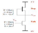
actually, i want design a NMOS inverter with these features : Picture14.png

so i must calculate the field oxide thickness for around the inverter .
 
Last edited:

hi

Vt= ∅_(MS )- Qox/Cox+ Qd/(Cox )+2∅_f

consider : vt = maximum voltge that may be placed on field oxide = 5v
and , Na = 1×10^15 1/cm^3 --> ∅_(MS ) = -.86 v

Qox=1×10^11×q=8×10^(-8 ) c/cm^2

∅_f=KT/q ln⁡(Na/ni)=0.0259ln⁡(1×10^15/1.5×10^10 )=0.288 v

Qd=2√(ε_0 ε_(si ) qNa∅_f )=2√(8.85×10^(-14 )×11.95×10^(15 )×1.6×10^(-19 )×.288)

Vt= -.86- (8×10^(-8 ))/Cox+ (1.39×10^(-8 ))/(Cox )+2×0.288=5

Cox= (1.39×10^(-8 )- 8×1^(-8 ) )/(5+ 0.86- 2×0.288)= -1.25×10^(-8 ) F/cm^2

Cox= (ε_0 ε_sio2 )/d

--> d= (5×8.85×10^(-14 )×3.9)/(1.25×10^(-8 ) )=1.38×10^(-4 ) cm=1.38μm

--> field oxide thickness = 1.38μm .

is it right ?
 

consider : vt = maximum voltge that may be placed on field oxide = 5v
Hi mojtaba,

1. the maximum voltage that may be placed on field oxide is not the threshold voltage of a field oxide MOSFET !
Even if your above calculations were correct (I didn't check them), you'd start from a wrong premise.

2. What for do you need the field oxide thickness at all? Your above shown inverter doesn't contain a field oxide transistor but a depletion transistor (I guess it's an NMOS), and such one uses the standard (thin) gate oxide - just a different channel implant. A field oxide NMOSFET would'nt work in this circuit configuration (would always be off).
____
BTW: A field oxide thickness of 1.38µm would be that of a very old process: a process size of 1.5 or 2µm had used such a thick field oxide, and such processes we had around 15..20 years ago.
 
thank you so much .

I think i need search and research much much more!

Excuse me , can you suggest me a good and update reference about ic fabriction ?
 

... can you suggest me a good and update reference about ic fabriction ?

Try the web sites of the "big" semiconductor fabs and foundries, like Intel, IBM, AMD, Samsung, TSMC, UMC, SMIC, ... and see which processes they offer.
 
Status
Not open for further replies.

Part and Inventory Search

Welcome to EDABoard.com

Sponsor

Back
Top