Continue to Site

Welcome to EDAboard.com

Welcome to our site! EDAboard.com is an international Electronics Discussion Forum focused on EDA software, circuits, schematics, books, theory, papers, asic, pld, 8051, DSP, Network, RF, Analog Design, PCB, Service Manuals... and a whole lot more! To participate you need to register. Registration is free. Click here to register now.

Even Page Address Boundary

Status
Not open for further replies.

electronicsman

Full Member level 5
Full Member level 5
Joined
May 4, 2012
Messages
291
Helped
11
Reputation
22
Reaction score
12
Trophy points
1,298
Activity points
3,737
This is the statement i have seen in the dspic33ev family reference manual. "The program memory must be erased at an “even” page address boundary."
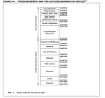
image.png
My calculations are 1 page is 8 rows, one row is 64 instructions hence 1 page = 8 * 64 = 512 instructions. As per the diagram the user flash memory starts at 0x000200. Hence the first page address falls at 0x000200 and the next page address falls at 0x000200 + 0x200 (512d) = 0x000400 and so on. Am I correct in this? Then what is this "even" page address boundary? Really confused. Please help.
 

I have written the following code to erase a page of flash memory. I have not yet started testing but please correct me if i made any mistake it will help me a lot. The compiler is XC16.
Code:
#include<xc.h>
/*
 * Program to erase a page of flash memory
 * family:dspic33ev256gm106
 */
_FOSCSEL(FNOSC_FRC & IESO_OFF);
_FOSC(FCKSM_CSECMD & OSCIOFNC_OFF & POSCMD_XT);
_FWDT(FWDTEN_OFF)
_FICD(ICS_PGD2)

#define MEMORY_PAGE_ERASE_OPERATION     (3u)
#define WREN                            (1 << 14)
#define NVMOP                           (MEMORY_PAGE_ERASE_OPERATION)
#define FLASH_PAGE_ERASE_CODE           (WREN | NVMOP)
#define SET                             (1u)

#define PM_ROW	__attribute__((space(prog), aligned(2)))

const PM_ROW eoldata_in_flash[10];
unsigned int nvmAdru;
unsigned int nvmAdr;
unsigned int nvmAdrPageAligned;

int main(int argc , char *argv[])
{
    
 PLLFBD=38;              // M=40
 CLKDIVbits.PLLPOST=1;   // N2=4
 CLKDIVbits.PLLPRE=0;    // N1=2 

// Initiate Clock Switch to Primary Oscillator with PLL (NOSC=0b011)
__builtin_write_OSCCONH(0x03);
__builtin_write_OSCCONL(OSCCON | 0x01);
// Wait for Clock switch to occur
while (OSCCONbits.COSC!= 0b011);
// Wait for PLL to locke
while (OSCCONbits.LOCK!= 1);
    /*step1  ---> set the NVMOP<3:0> to erase the page of flash program memory */
    NVMCON = FLASH_PAGE_ERASE_CODE;
    /*step2: write the starting address of the page to be erased into NVMADRU and NVMADR registers */
    nvmAdru=__builtin_tblpage(&eoldata_in_flash[0]);
	nvmAdr=__builtin_tbloffset(&eoldata_in_flash[0]);
	nvmAdrPageAligned=nvmAdr & 0xFC00;			/* Get the Flash Page Aligned address */
    NVMADRU = nvmAdru;
    NVMADR = nvmAdrPageAligned;
    /*step3: with interrupts disabled write the key sequence */
    __builtin_write_NVM();
    /* set the WR bit it will start erase operation */
    NVMCONbits.WR = SET;
    while(1);
    return 0;
}
 

Status
Not open for further replies.

Similar threads

Part and Inventory Search

Welcome to EDABoard.com

Sponsor

Back
Top