Continue to Site

Welcome to EDAboard.com

Welcome to our site! EDAboard.com is an international Electronics Discussion Forum focused on EDA software, circuits, schematics, books, theory, papers, asic, pld, 8051, DSP, Network, RF, Analog Design, PCB, Service Manuals... and a whole lot more! To participate you need to register. Registration is free. Click here to register now.

ESP8266 & LoRa Design - Opinions?

Status
Not open for further replies.

5spdvl

Newbie
Joined
May 11, 2022
Messages
3
Helped
0
Reputation
0
Reaction score
0
Trophy points
1
Activity points
49
Hello all,

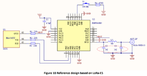
I've designed a portable LoRa module, operated by an ESP8266 module, powered by a lipo and recharged over USB-C. Attached is the EasyEDA schematic.
I've spent a few years tinkering with the major components of this design as discrete units (like, a ESP8266 NodeMCU dev board, rather than the module itself), but I am really wanting to be able to design PCBs from scratch. The attached design was created using the datasheets for each component, and my understanding of electronics.

I am a hobbyist, so there are no doubt errors or odd choices. Seeking feedback to improve/avoid a lipo overcharge situation 🔥

Thankyou.

Schematic_LoRa-E5 Tracker_2022-05-11.png
 

Hi,

Most of the schematic is good.
But there are things to change for the future:
* no signals through symbols
* no lenghty GND wires, use GND symbol instead
* the same for VCC
* avoid the 4x 90° angles when signals cross
* I see all your symbols are drawn with the pin order like on the PCB. It's not the job of a schematic to show the "mechanical" situation. Better place them to get an easy readable schematic.

I can't imagine what H1 could be ... and how this wiring could be right. Please explain.
I don't think 2x 0.1uF at the antenna is correct
Currently your battery can only be charged when the power switch is ON. Is this what you want?
U1_PB13 has internal pull up?
I see no need for series resistors like R2 ... but they don't harm.
Rx an Tx lines are rather important signal lines. But they directly drive LEDs. Are you sure they maintain good LOW levels (including good noise margin)?
You drive all VCC via D1. This causes a lot of voltage drop, do you want this? And check that the VCC current is below the diode specification in any case.
The standard power supply decoupling capacitor is 100nF ceramics. Mind that 4u7 ... 22u are usually much slower. Especially in case of C5 I recommend to add a fast capacitor.
Some pins need valid signal levels (on power up). Check all pins.
Mind: no pin/signal should be left floating (unless specified differently).
H2 seems to be a connector --> shouldn't it be X2 (use correct designators)
H2 also is named as I2C. I miss valid pull up resistors. Check on this.
LED6 (maybe LED3, too) draw battery current and can't be switched OFF. This reduces battery lifetime ... and makes deep power down impossible.
Check which signals (entering/leaving the PCB) need ESD protection. (I2C comes to my mind)

Most of the above are no "real mistakes" .. just my ideas / recommendations.

****
PCB layout:
Especially for beginners I strongly recommend to use a layer just for GND. Solid, no other traces.
This makes wiring more easy (just a via at every GND pin ... and forget about it) and gives stable, reliable operation.
Don't be afraid of using 4 layers.

You are using HF (LoRa), high speed sensitive signals, switching power signals .. all on one PCB. This calls for trouble ... when not experienced. With a solid GND plane you are on the save side. Once you are more experienced in PCB routing you are able to reduce layoer count to save money on mass production..

Sporadic reset, sending out noise or receiving noise (EMI/EMC) are problems without a solid GND plane.

Klaus
 

Thanks KlausST, I appreciate you taking the time to provide detailed feedback!

To answer your questions:

H1 is intended to be a UART connector, for programming the ESP8266 in the absence of a CP210x, etc. The idea is that the battery would be switced off at SW1, the module would then take 3V3, GND, TX/RX through that connector - only during programming. The diode at D1 is there to prevent power from H1 going back into U8 (AMS1117-3.3).

Good point re: C2 & C3 - they are there as is shown in the reference diagram for the datasheet of the LoRa-E5 module, however they don't specify a value (and actually says "NC", despite beeing connected to GND). See attached reference diagram.

That is fine re: charging only when SW1 is on - designed as a safety to disconnect the battery/turn off the module.

PB13 internal pullup - again, I've followed the attached referenced diagram. It doesn't specify anything about it.

R2 - reference diagram again.

RX/TX driving LEDs - in my own testing with an ESP8266 NodeMCU dev board, wiring LEDs as per my schematic makes them fuction as visual indicators (which is their purpose in the schematic). However I don't know of a way to test if this would cause issue for communication between the uCs. I guess I could try setting up serial comms between 2x ESPs with LEDs and see if it affects it? Or perhaps there's a better way to indicate comms activity.

I believe D1 & D2 have a rating of 500mA - the total for th circuit shouldn't exceed that, if I've checked everything correctly. The purpose of those diodes it to protect from voltage running into components the wrong by meforgetting to unplug USB-C charging power whilst UART power is connected, or vice versa. There is probably a better way to provide this protection, but I havem't been able to work that out as yet.

Decoupling caps - the FP6277 specifies a 22uF, and the AS1117-3.3 was a bit hard to get a good consensus on the right value; only one datasheet specified a 10uF, and that was for thermal characteristic testing. I can certainly reduce their values.

I've been over it several times to confirm the high/low status for (at least) the ESP - they seem ok. Well, they match what I've researched and tested.

Floating pins - LoRA-E5 datasheet specifically states that PB0 must be left floating, all others have no requirements. Are you saying that unused pins should be tied to ground?

H2 is a header for (possible) I2C hardware at a later stage - I'll add some 10K pullups between SDA/SCL and 3V3. Or would 100K be better, given it's a battery powered device?

Good point re: battery LED. Will consider deleting it or making it switchable.

Re: ESD; How would I go about that? I know there are ESD protection diodes, such as the TPD1E10B06, which you could connect between the signal line and GND - is this a good method? And that would mean putting them on RX/TX and SDA/SCL?


I certainly appreciate your point re: PCB design and not utilising a ground plain. The actual PCB side of things is a whole different game! :oops:

Thanks again.
 

Attachments

  • Untitled.png
    Untitled.png
    135.6 KB · Views: 127

Hi
H1 is intended to be a UART connector, for programming the ESP8266 in the absence of a CP210x, etc. The idea is that the battery would be switced off at SW1, the module would then take 3V3, GND, TX/RX through that connector - only during programming. The diode at D1 is there to prevent power from H1 going back into U8 (AMS1117-3.3).
I see. If you have the space, then I recommend to add all for uploading necessary signals to the connector (RESET, EN, BOOT ...)
Mind the ESD protection. If you connect the programming cable, and here is an ESD damage, then this does not necessarily means an immediate fail. ESD problems can cause a fail in the field even after months.

1N4148 is rated for 200mA only and it has a voltage drop of 1V @200mA ... remaining just 2.3V .. what should be 3.3V.
I smell some trouble...

Check if the AM1117 has a problem at all when the output is driven with 3.3V.

That is fine re: charging only when SW1 is on - designed as a safety to disconnect the battery/turn off the module.
Two points to consider:
* even if the switch is OFF then device won´t be OFF when charger is powered.
* how does the charger output behave when there is no battery? Low voltage, high voltage, pulsing????

RX/TX driving LEDs
No need for testing, no need for guessing. Just read the datasheets and check whether the voltage levels are in a valid region with the expected current.
A functional test wil not give any reliability. It may vary with the part, time, temperature, supply voltage...
--> if it´works on one situation .. there is no guarantee that it works in either situation.
If test, then a "worst case test" (lowest supply voltage, various temperatures, good margin...)

I believe D1 & D2 have a rating of 500mA
For me speaking: "I believe" is a no-go for reliable designs. I have to be sure, thus a read a lot of datasheets.
As already written: "200 mA". And you have to consider all situations. During programming, during boot, during transmitting, all LEDs ON, lowest expectable supply voltage... --> worst case.
2.3V instead of 3.3V ... Are you sure?

Capacitors:
Not only the pure uF value is of interest, but also their ESR over frequency. (besides voltage ...)
IC manufacturers provide information in the datsheets and application notes. I recommend to read them.

Are you saying that unused pins should be tied to ground?
No. The must not left floating.
* they may be pulled internally
* they may have a "keeper" internally
* thay may be pulled externally with (or without) resistors
* port pins may be programmed not to float
* maybe other methods

Floating pins a prone to pick up noise (sporadic misfunction), may oscillate, may cause increased supply current...

***
I2C pullup:
Does not (primarily) depend on supply current. They are installed for proper function of I2C communication. As long as the I2C is not active they don´t draw current anyways. I´d use 10k as the upper limit.

Indeed the total supply current may be less with installed pullup because it prevents from flaoting pin, which may cause crowbar current in the input stage.

***
ESD protection:
Used dedicated ESD diodes. I recommend on each signal that enters/leaves the PCB.

*****
I know it might be boring / annoying when I refer to datasheets and application notes. But I see it as the only way to prevent from "bad surprise". I do it every day. many many pages.

Klaus
 

One small point R3 10K connected to the RST line on the ESP8266 does not do anything, the ESP8266 has internal pull ups enabled and 10K is much to high to over come the pull up. You should reduce the value to 1K if you want a reset pulse on power up.
On the original firmware of the ESP8266 the pull ups were not enabled but they have been now for many years, I was caught out by this myself.
 

Thanks for that, pjmelect - the reference diagram I was using was dated 2016, and I've just read about the ESP8266 firmware being updated to enable the internal pullups. I'll make that change.

Thanks KlausST; I've added some ESD protection diodes on signals lines (RX/TX, SDA/SCL), and some pullup resistors on the SDA/SCL lines (4k7).
 

Status
Not open for further replies.

Similar threads

Part and Inventory Search

Welcome to EDABoard.com

Sponsor

Back
Top