Continue to Site

Welcome to EDAboard.com

Welcome to our site! EDAboard.com is an international Electronics Discussion Forum focused on EDA software, circuits, schematics, books, theory, papers, asic, pld, 8051, DSP, Network, RF, Analog Design, PCB, Service Manuals... and a whole lot more! To participate you need to register. Registration is free. Click here to register now.

EFR32FG14 SPI Chip Select problem

Status
Not open for further replies.
Hi,

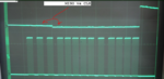
Time flow in a scope picture is left to right.

Thus I fully agree with Susan. What you call "rising edge" indeed is "falling edge".

Klaus
 

I don't understand the purpose of the "data flow" annotation. In my view it's confusing the straightforward SPI protocol specification. The waveforms are showing regular SPI mode 0, clock idles low, data expected to be read on the rising clock edge. I'm sure you can understand it by reading the specification thoroughly.
--- Updated ---

You need of course to verify that the slave chip is also "understanding" mode 0. That's the case for the memory chips discussed above.
 
Last edited:

I'm not familiar with the exact device but in a previous post it was pointed out that the command (0x06) should be sent independently of the the data. To my mind, and based on working software I have written in the past, that means 'SYNC' has to be raised (de-select) after the command byte then reasserted for the data following it. Just adding 0x06 before the data will not make the device respond.

Perhaps the point being missed is that the 'SYNC' or '-CS' or whatever it is called is used to indicate the start of a transaction and also to mark the end of the transaction, the end usually latching the serial bits into the device in parallel. A transaction here meaning a command, read or write operation.

Brian.
 

The datasheet is clearly indicating the number of bytes to be send with each command. WREN (0x06) is a single byte command and as stated, only valid if nCS is raised after it. Respectively, a succeeding command is only recognized if sent directly after nCS pulled low.
 

I must admit that I have NEVER heard of an oscilloscope that scans right to left.
I therefore interpreted your image in the conventional left to right order.
Susan
 

Hello,Thank you for the scope intuittion, Tommorow i will present all three commands on the scope data vs clk ,data vs chip select with the logic from the manual.
Thanks.
 

Hello, I am using efr32fg14 starter kit board in which i am trying to write value E6 into address HEX 00,00,00,00 in mx25R device which manual shown bellow.i am using for that 3 commands
{0x06};//write enable command
{0x02,0x00,0x00,0x00,0x00,0xE6}; //write to all zero register the value E6
as shown in the full updated code bellow.
A numerated photos shown bellow of the data vs clk ,clk vs chip select of ech command and the MISO response which is a straight VDD line instead of
E6 shape which is 11100110
Where did i go wrong?
Thanks.
**broken link removed**

1.jpeg


2.jpeg

3.jpeg

4.jpeg

5.jpeg

6.jpeg

7.jpeg

8.jpeg

9.jpeg

10.jpeg


Code:
/**************************************************************************//**
 * @main_series1_PG1_EFR.c
 * @brief Demonstrates USART1 as SPI master.
 * @version 0.0.2
 ******************************************************************************
 * @section License
 * <b>Copyright 2018 Silicon Labs, Inc. http://www.silabs.com</b>
 *******************************************************************************
 *
 * This file is licensed under the Silabs License Agreement. See the file
 * "Silabs_License_Agreement.txt" for details. Before using this software for
 * any purpose, you must agree to the terms of that agreement.
 *
 ******************************************************************************/

#include <stdint.h>
#include <stdbool.h>
#include "bsp.h"
#include "bsp_trace.h"


#include "em_emu.h"


#include "em_device.h"
#include "em_chip.h"
#include "em_cmu.h"
#include "em_gpio.h"
#include "em_usart.h"
#include "em_ldma.h"

#define TX_WREN_BUFFER_SIZE   1
#define TX_WRITE_BUFFER_SIZE   6
#define TX_READ_BUFFER_SIZE   5

#define RX_BUFFER_SIZE   1


uint8_t Tx_WREN[TX_WREN_BUFFER_SIZE] = {0x06};//write enable command
uint8_t Tx_PP[TX_WRITE_BUFFER_SIZE] = {0x02,0x00,0x00,0x00,0x00,0xE6}; //write to all zero register the value E6
uint8_t Tx_READ[TX_READ_BUFFER_SIZE] = {0x03,0x00,0x00,0x00,0x00}; //read register 00,00,00,00

uint32_t TxBufferIndex = 0;

uint32_t RxBuffer;
//uint32_t RxBufferIndex = 0;

volatile uint32_t msTicks; /* counts 1ms timeTicks */

void Delay(uint32_t dlyTicks);

void SysTick_Handler(void)
{
  msTicks++;       /* increment counter necessary in Delay()*/
}
void Delay(uint32_t dlyTicks)
{
  uint32_t curTicks;

  curTicks = msTicks;
  while ((msTicks - curTicks) < dlyTicks) ;
}
int main(void)
{
     CHIP_Init();
    CMU_ClockEnable(cmuClock_GPIO, true);
        CMU_ClockEnable(cmuClock_USART1, true);
        CMU_ClockEnable(cmuClock_USART0, true);

        // Configure GPIO mode
        GPIO_PinModeSet(gpioPortC, 8, gpioModePushPull, 0); // US1_CLK is push pull
        GPIO_PinModeSet(gpioPortA, 4, gpioModePushPull, 1); // US1_CS is push pull
        GPIO_PinModeSet(gpioPortC, 6, gpioModePushPull, 1); // US1_TX (MOSI) is push pull
        GPIO_PinModeSet(gpioPortC, 7, gpioModeInput, 1);    // US1_RX (MISO) is input

        // Start with default config, then modify as necessary
        USART_InitSync_TypeDef config = USART_INITSYNC_DEFAULT;
        config.master       = true;            // master mode
        config.baudrate     = 1000000;         // CLK freq is 1 MHz
        config.autoCsEnable = false;            // CS pin controlled by firmware, not hardware
        config.clockMode    = usartClockMode0; // clock idle low, sample on rising/first edge
        config.msbf         = true;            // send MSB first
        config.enable       = usartDisable;    // Make sure to keep USART disabled until it's all set up
        USART_InitSync(USART1, &config);

        USART_InitAsync_TypeDef init = USART_INITASYNC_DEFAULT;

        // set pin modes for UART TX and RX pins
          GPIO_PinModeSet(gpioPortA, 1, gpioModeInput, 1);
          GPIO_PinModeSet(gpioPortA, 0, gpioModePushPull, 1);
          ///////////////////////////////////

            USART_InitAsync(USART0, &init);

            USART0->ROUTELOC0 =(USART_ROUTELOC0_TXLOC_LOC0)  | // US1_TX (MOSI) on location 11 = PC6 per datasheet section 6.4 = EXP Header pin 4
           (USART_ROUTELOC0_RXLOC_LOC0);   // US1_RX (MISO) on location 11 = PC7 per datasheet section 6.4 = EXP Header pin 6

        // Set USART pin locations
        USART1->ROUTELOC0 = (USART_ROUTELOC0_CLKLOC_LOC11) | // US1_CLK       on location 11 = PC8
                            (USART_ROUTELOC0_CSLOC_LOC11)  | // US1_CS        Manual
                            (USART_ROUTELOC0_TXLOC_LOC11)  | // US1_TX (MOSI) on location 11 = PC6
                            (USART_ROUTELOC0_RXLOC_LOC11);   // US1_RX (MISO) on location 11 = PC7

        // Enable USART pins
        USART1->ROUTEPEN = USART_ROUTEPEN_CLKPEN  | USART_ROUTEPEN_TXPEN | USART_ROUTEPEN_RXPEN;
        // Enable USART1
           USART_Enable(USART1, usartEnable);
           TxBufferIndex = 0;

           if (SysTick_Config(CMU_ClockFreqGet(cmuClock_CORE) / 1000)) {
                 while (1) ;
               }

           while(1)
     {

              Delay(1);
              GPIO_PinOutClear(gpioPortA,4);
               USART_SpiTransfer(USART1,Tx_WREN[0]);
            GPIO_PinOutSet(gpioPortA,4);

              Delay(1);
                GPIO_PinOutClear(gpioPortA,4);
                   USART_SpiTransfer(USART1,Tx_PP[0]);
                  USART_SpiTransfer(USART1,Tx_PP[1]);
                  USART_SpiTransfer(USART1,Tx_PP[2]);
                  USART_SpiTransfer(USART1,Tx_PP[3]);
                  USART_SpiTransfer(USART1,Tx_PP[4]);
                  USART_SpiTransfer(USART1,Tx_PP[5]);
                 GPIO_PinOutSet(gpioPortA,4);
                Delay(1);
                //Tx_READ
               GPIO_PinOutClear(gpioPortA,4);
              USART_SpiTransfer(USART1,Tx_READ[0]);
             USART_SpiTransfer(USART1,Tx_READ[1]);
             USART_SpiTransfer(USART1,Tx_READ[2]);
             USART_SpiTransfer(USART1,Tx_READ[3]);
             USART_SpiTransfer(USART1,Tx_READ[4]);
               GPIO_PinOutSet(gpioPortA,4);


             }

}
--- Updated ---

Photos 11 to 15 for the attached files in post before.
11.jpeg

12.jpeg

13.jpeg

14.jpeg

15.jpeg
 

Hi,
{0x02,0x00,0x00,0x00,0x00,0xE6}; //write to all zero register the value E6
Please use the terminology "address".
If I understand correct, then you want to write "0xE6" into address "0x000000"

so the complete command should be (please refer to Fig. 30)
{0x02,0x00,0x00,0x00,0xE6}
0x02 (command "PP")
0x000000 (24 bit address)
0xE6 (data)

btw: you are free to use paper and colored pencils on your own ;-)

but your sequence:
{0x02,0x00,0x00,0x00,0x00,0xE6}
where does the red "0x00" come from?

What happens with your command:
0x00 gets written in to address 0x000000
0xE6 gets written in to address 0x000001 (the address folowing to 0x000000)

Klaus
 

The suggested datasheet page program sequence is reading status register to assure that all prerequisites for writing to the flash are met. This way conditions like active WP pin or locked blocks can be detected.
--- Updated ---

Page program cycle time is specified with typ. 3.2 ms, max 10 ms. As you are only waiting 1 ms, write is most likely not terminated when you perform read.
 
Last edited:

Hello VFM,Thank you very much,So its desighned to work when i send the commands 1ms delay between each SPI command and if i understand correctly the writing sequence will work. after which the reading will be done.
Klauss thanks alot,You are correct 24bits is 3 bits not 4. So its 00,00,00 address . i will UPDATE as soon as possible.
 

Don't use timing to tell when the write cycle completes - the WIP bit will tell you. Read the status register (which doesNOT stop the write cycle) until the "WIP" bit goes to 0 and then do the read.
Susan
 

Or, for a simplified test, wait 10 ms.

It's not good to write the same memory location repeatedly without previously erasing the page.
 

Hello,I have added the Chip erase command and the read status commands also i removed the while loop only one stear of commands .
I have reduced the delay between the commands from 1ms to much less using GPIO set clear for loops.
but my MISO from where i am supposed to see the result of the read status and the READ command i am getting undefined behavior as shown in the enumerated photos of DATA vs CLK (each command separately ) and CS vs CLK ,and MISO vs CLK.
The full code is also ettached .
where did i go wrong?
Thanks.
1.jpeg
2.jpeg
3.jpeg
4.jpeg
5.jpeg
6.jpeg
7.jpeg
8.jpeg
9.jpeg

Code:
/**************************************************************************//**
 * @main_series1_PG1_EFR.c
 * @brief Demonstrates USART1 as SPI master.
 * @version 0.0.2
 ******************************************************************************
 * @section License
 * <b>Copyright 2018 Silicon Labs, Inc. http://www.silabs.com</b>
 *******************************************************************************
 *
 * This file is licensed under the Silabs License Agreement. See the file
 * "Silabs_License_Agreement.txt" for details. Before using this software for
 * any purpose, you must agree to the terms of that agreement.
 *
 ******************************************************************************/

#include <stdint.h>
#include <stdbool.h>
#include "bsp.h"
#include "bsp_trace.h"


#include "em_emu.h"


#include "em_device.h"
#include "em_chip.h"
#include "em_cmu.h"
#include "em_gpio.h"
#include "em_usart.h"
#include "em_ldma.h"

#define TX_WREN_BUFFER_SIZE   1
#define TX_WRITE_BUFFER_SIZE   5
#define TX_READ_BUFFER_SIZE   4

#define RX_BUFFER_SIZE   1


uint8_t Tx_WREN[TX_WREN_BUFFER_SIZE] = {0x06};//write enable command
uint8_t Tx_CHIP_ERASE[TX_WREN_BUFFER_SIZE] = {0xC7};//Chip Erase
uint8_t Tx_READ_STATUS[TX_WREN_BUFFER_SIZE] = {0x05};//read status
uint8_t Tx_PP[TX_WRITE_BUFFER_SIZE] = {0x02,0x00,0x00,0x00,0xE6}; //write to all zero register the value EF
uint8_t Tx_READ[TX_READ_BUFFER_SIZE] = {0x03,0x00,0x00,0x00}; //read register 00,00,00,00

uint32_t TxBufferIndex = 0;

uint32_t RxBuffer;
//uint32_t RxBufferIndex = 0;

volatile uint32_t msTicks; /* counts 1ms timeTicks */

void Delay(uint32_t dlyTicks);

void SysTick_Handler(void)
{
  msTicks++;       /* increment counter necessary in Delay()*/
}
void Delay(uint32_t dlyTicks)
{
  uint32_t curTicks;

  curTicks = msTicks;
  while ((msTicks - curTicks) < dlyTicks) ;
}
int main(void)
{
    int i;
     CHIP_Init();
    CMU_ClockEnable(cmuClock_GPIO, true);
        CMU_ClockEnable(cmuClock_USART1, true);
        CMU_ClockEnable(cmuClock_USART0, true);

        // Configure GPIO mode
        GPIO_PinModeSet(gpioPortC, 8, gpioModePushPull, 0); // US1_CLK is push pull
        GPIO_PinModeSet(gpioPortA, 4, gpioModePushPull, 1); // US1_CS is push pull
        GPIO_PinModeSet(gpioPortA, 5, gpioModePushPull, 1); // delay gpi
        GPIO_PinModeSet(gpioPortC, 6, gpioModePushPull, 1); // US1_TX (MOSI) is push pull
        GPIO_PinModeSet(gpioPortC, 7, gpioModeInput, 1);    // US1_RX (MISO) is input

        // Start with default config, then modify as necessary
        USART_InitSync_TypeDef config = USART_INITSYNC_DEFAULT;
        config.master       = true;            // master mode
        config.baudrate     = 1000000;         // CLK freq is 1 MHz
        config.autoCsEnable = false;            // CS pin controlled by firmware, not hardware
        config.clockMode    = usartClockMode0; // clock idle low, sample on rising/first edge
        config.msbf         = true;            // send MSB first
        config.enable       = usartDisable;    // Make sure to keep USART disabled until it's all set up
        USART_InitSync(USART1, &config);

        USART_InitAsync_TypeDef init = USART_INITASYNC_DEFAULT;

        // set pin modes for UART TX and RX pins
          GPIO_PinModeSet(gpioPortA, 1, gpioModeInput, 1);
          GPIO_PinModeSet(gpioPortA, 0, gpioModePushPull, 1);
          ///////////////////////////////////

            USART_InitAsync(USART0, &init);

            USART0->ROUTELOC0 =(USART_ROUTELOC0_TXLOC_LOC0)  | // US1_TX (MOSI) on location 11 = PC6 per datasheet section 6.4 = EXP Header pin 4
           (USART_ROUTELOC0_RXLOC_LOC0);   // US1_RX (MISO) on location 11 = PC7 per datasheet section 6.4 = EXP Header pin 6

        // Set USART pin locations
        USART1->ROUTELOC0 = (USART_ROUTELOC0_CLKLOC_LOC11) | // US1_CLK       on location 11 = PC8
                            (USART_ROUTELOC0_CSLOC_LOC11)  | // US1_CS        Manual
                            (USART_ROUTELOC0_TXLOC_LOC11)  | // US1_TX (MOSI) on location 11 = PC6
                            (USART_ROUTELOC0_RXLOC_LOC11);   // US1_RX (MISO) on location 11 = PC7

        // Enable USART pins
        USART1->ROUTEPEN = USART_ROUTEPEN_CLKPEN  | USART_ROUTEPEN_TXPEN | USART_ROUTEPEN_RXPEN;
        // Enable USART1
           USART_Enable(USART1, usartEnable);
           TxBufferIndex = 0;

           if (SysTick_Config(CMU_ClockFreqGet(cmuClock_CORE) / 1000)) {
                 while (1) ;
               }

    //       while(1)
    // {

                                      for(i=0;i<200;i++)
                                      {
                                      GPIO_PinOutSet(gpioPortA,5);

                                          GPIO_PinOutClear(gpioPortA,5);
                                            }

              GPIO_PinOutClear(gpioPortA,4);
               USART_SpiTransfer(USART1,Tx_WREN[0]);
            GPIO_PinOutSet(gpioPortA,4);

                                                 for(i=0;i<10;i++)
                                                  {
                                                  GPIO_PinOutSet(gpioPortA,5);

                                                      GPIO_PinOutClear(gpioPortA,5);
                                                        }
         GPIO_PinOutClear(gpioPortA,4);
         USART_SpiTransfer(USART1,Tx_CHIP_ERASE[0]);
         GPIO_PinOutSet(gpioPortA,4);
                                                    for(i=0;i<10;i++)
                                                          {
                                                          GPIO_PinOutSet(gpioPortA,5);
                                                              GPIO_PinOutClear(gpioPortA,5);
                                                                }


         GPIO_PinOutClear(gpioPortA,4);
                 USART_SpiTransfer(USART1,Tx_READ_STATUS[0]);
                 GPIO_PinOutSet(gpioPortA,4);
                                                            for(i=0;i<10;i++)
                                                                  {
                                                                  GPIO_PinOutSet(gpioPortA,5);
                                                                      GPIO_PinOutClear(gpioPortA,5);
                                                                        }


                GPIO_PinOutClear(gpioPortA,4);
                   USART_SpiTransfer(USART1,Tx_PP[0]);
                  USART_SpiTransfer(USART1,Tx_PP[1]);
                  USART_SpiTransfer(USART1,Tx_PP[2]);
                  USART_SpiTransfer(USART1,Tx_PP[3]);
                  USART_SpiTransfer(USART1,Tx_PP[4]);
                 GPIO_PinOutSet(gpioPortA,4);
                                                        for(i=0;i<10;i++)
                                                               {
                                                               GPIO_PinOutSet(gpioPortA,5);
                                                                   GPIO_PinOutClear(gpioPortA,5);
                                                                     }

                GPIO_PinOutClear(gpioPortA,4);
                                USART_SpiTransfer(USART1,Tx_READ_STATUS[0]);
                                GPIO_PinOutSet(gpioPortA,4);
                                                   for(i=0;i<10;i++)
                                                      {
                                                      GPIO_PinOutSet(gpioPortA,5);
                                                          GPIO_PinOutClear(gpioPortA,5);
                                                            }

               GPIO_PinOutClear(gpioPortA,4);
              USART_SpiTransfer(USART1,Tx_READ[0]);
             USART_SpiTransfer(USART1,Tx_READ[1]);
             USART_SpiTransfer(USART1,Tx_READ[2]);
             USART_SpiTransfer(USART1,Tx_READ[3]);

               GPIO_PinOutSet(gpioPortA,4);


      //       }//end while(1)

}
 

Hi,

It seems you read the statsus byte .. but don´t care about it´s state.

With 0x05 it says the write process is still acitve...

You urgently need to read the datasheet and follow it´s


I´ll try with an example to explain what you do:
Let´s say you want to send a parcel with a bottle of tea to your friend.
The bottle now has unknown content.
Before you send the pacel you turn the bottle to empty it.
You neither check whether the bottle is empty nor do you spend enough time for the bottly to empty completely. (mistake 1)
You immediatley turn it around and try to fill in tea.
What will happen? With some luck the bottle was empty and can be filled with tea. With less luck there may be a mixture of something and your tea in the bottle. or maybe no tea at all.

Then you send the parcel.
You check the delivery status. It says the parcel is still on it´s way.
--> You don´t care about the delivery status "still on it´s way" nor do you give the parcel enough time to arrive.. (mistake 2)
Instead you immediately call your friend and ask what´s in the bottle.

What will be the answer? Surely he/she does not know yet....


Klaus
 

Hello Klauss,From the manual shown bellow ,as a reaction to the read status command ,i need to see an 8 bit status data where bit0 and bit0 in the data on the MISO is the WEL and WIP.
But i dont see in the in the MISO LINE bellow a valid data.
After the clear chip command the WIP should have been 1 to show that its busy erasing chip.
But we see logic 1 only after the last command.
Why my MIso line doesnt react to the read status commands?
Thanks.
1600083600553.png

1600083748229.png
1600081214616.png


1600079794104.png
 

Attachments

  • 1600079687579.png
    1600079687579.png
    1.2 MB · Views: 81
  • 1600079890153.png
    1600079890153.png
    85.8 KB · Views: 64
  • 1600080010796.png
    1600080010796.png
    85.8 KB · Views: 75
Last edited:

Hi,

I don´t like to seek through all your code.

So what´s your READ_STATUREGISTER sequence?

I see only 0x05 (1 byte) ... but according the datashheet the command needs 3 bytes....
(sorry: 2 bytes, but you may repeatedly read the startusregister until the chip is IDLE)

I still don´t see the timing (according datsheet) to wait after ERASE or WRITE to the IC.

--> If you don´t read and follow the datasheet then it takes too much time for us to explain every single step.
We need (and do) read your datasheet, too. I´v never worked with this IC ... all I know is from the datsheet you posted..

Klaus
 

Hello Klauss thank you very much for our effort to help me,i am doing my best to show my logic based on the manual.
I understood my error previosly,I need to use the recieve command shown bellow and use endless loop till it shows that its completed the command
uint8_t USART_Rx(USART_TypeDef *usart)

How did you see we need three bytes for read status? from the manual page 18, its only one byte command.
Thanks.
**broken link removed**
1600088536058.png
 

Attachments

  • 1600088444483.png
    1600088444483.png
    61.7 KB · Views: 82

Hi,

it shows:

Action:
* 1 byte command 0x05
* then read out the status register.
Maybe not very clear for a beginner who is just after a fast solution (Hope you don´t mind that I assume this).
I would not be surprised if it becomes frustrating and slow..
If you see Figure 11 then every thing should be clear. Or if you know SPI basics)

I recommend to do first things first. Learn basics, draw flow charts, write simple SPI functions, verify them, write the more complex SPI functions, verify them.

Your microcontroler is the SPI_master, it needs to provide 8 clock cycles to read the (status register... and any other) contents.
...as with all SPI communications...
These 8 clock cycles are missing.
A usual way to generate those 8 clock cycles is to send a dummy byte (as SPI is a full duplex serial interface). It does not matter what dummy byte value you send.

Figure 11 is rather clear with this.:
* SPI_Master needs to set CS = LOW
* then SPI master sends out the command byte 0x05 ... by sending 8 clock cycles
* then the master needs to send yout 8 clock cycles for reading the data (status) byte
* the master is free to read the status byte many times -- as long as CS is held LOW.

This is nothing special, rather common for SPI communcation.
If you are not familiar with standard SPI communication, then please read tutorials.

In the datasheet there is
* a textual description .. to explain how everything works.
* a flow chart ... to write and check your software
* a timing diagram to .... compare your scope picture
this is more than one can expect.. Other datasheets show only one method....


Klaus
 

Hello Klauss,Yes i noticed that after the transfer function is completed then the CLK signal just stops.
And as you said correctly we need for the clock to continue. so what you are saying that we have to use
uint8_t USART_Rx(USART_TypeDef *usart)
because the slave device will not send a response without having a clock signal.
If i understand your words correctly i will try and make a simple Write enable command where we expect bit1 (WEL=1) and rest is zero.
and read this status only.

I will try to implement it and update later.
Thanks
 

Hi,

Yes i noticed that after the transfer function is completed then the CLK signal just stops.
"You noticed" .. this is the first step to progresss .. but the next step should be not to ignore it, but to find out "why".
Don´t continue to code other functions, don´t do random changes on your code.

I want you to to make progress, to find debugging methods on your own...
I recommend to write a piece of code then - before testing - write down as detailed as possible what you expect. Here a timing diagram should be useful.
Then connect the scope and test the code. Verify the scope picture with your expectation. Be critical. If there are just 8 clock cycles when you expect 16 clock cycles then ask yourself how this can be.
If you know that only the SPI_master is responsible for sending clocks, then you know the SPI_master is doing something wrong.
Then verify your code ... what happens (in your code) immedialtely after sending the first 8 clocks?
--> oops - nothing that tells to send another 8 bits.
so the solution is to make it send out another 8 clocks.
*************

I don´t know what "uint8_t USART_Rx(USART_TypeDef *usart) " does, because I don´t have a documentation about this function.
But I don´t think I need it - but you should be familiar with it.

************

Yes. Start with simple code. Code that you can verify. Either with a scope, or with known return values.

READ STATUS .... WRITE WEL .... READ STATUS
to see how the STATUS changes.

Klaus
 

Status
Not open for further replies.

Part and Inventory Search

Welcome to EDABoard.com

Sponsor

Back
Top