Continue to Site

Welcome to EDAboard.com

Welcome to our site! EDAboard.com is an international Electronics Discussion Forum focused on EDA software, circuits, schematics, books, theory, papers, asic, pld, 8051, DSP, Network, RF, Analog Design, PCB, Service Manuals... and a whole lot more! To participate you need to register. Registration is free. Click here to register now.

Eagle: IC pad design

Status
Not open for further replies.

PRASAN DUTT RAJU

Junior Member level 1
Joined
Jun 14, 2012
Messages
18
Helped
0
Reputation
0
Reaction score
0
Trophy points
1,281
Activity points
1,410
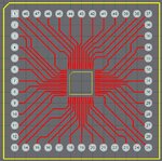
I'm designing the PBC layout of IC LPC1343 only its dedicated pad. But after going through all the process I'm stuck at Autorouter step as it is not able to optimize the the design. First I thought there may be reason that I've not given supply voltage & Ground that's why its not working but after adding both of two in schematic, once again the same problem has raised. It shows like this IC pad layout.jpg
My final layout should look like thislpc1343Adaptor.JPG.
 

My guess is that your autorouter setup is wrong.

1) Fine-pitch components should be aligned with the grid (all pads);

2) Routing grid should be (at least) equal the pitch of fine-pitch
components. If the pitch is not an exact routing grid multiple (ex.:
pitch=0.50mm and routing grid = 0.25mm), then you need a very small routing grid
to route the PCB.

3) DRC clearance should be smaller than the pitch minus the trace width
(space is needed for the trace to get to the pad). At least for the
clearance between the wires it should be in accordance to this rule.

Also have a look at this site:
https://intranet.ee.ic.ac.uk/t.clarke/eagle/Eagle_configuration.htm
 
I used manual routing because it's only 48 pin routing. However I've changed the shape. 1075086_10200432509960943_696356855_n.jpg
Now after production it's looking & working fine.
 

Status
Not open for further replies.

Part and Inventory Search

Welcome to EDABoard.com

Sponsor

Back
Top