Continue to Site

Welcome to EDAboard.com

Welcome to our site! EDAboard.com is an international Electronics Discussion Forum focused on EDA software, circuits, schematics, books, theory, papers, asic, pld, 8051, DSP, Network, RF, Analog Design, PCB, Service Manuals... and a whole lot more! To participate you need to register. Registration is free. Click here to register now.

driver compression logic

yefj

Advanced Member level 4
Joined
Sep 12, 2019
Messages
1,237
Helped
1
Reputation
2
Reaction score
3
Trophy points
38
Activity points
7,444
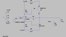
Hello, I have the following circuit where the heart is the BJT.when i put the resistor to be 50Ohms i get a good sine current on the inductor L1 shown below.
But when i put 25 ohms i get compression .
In the compressed version i see that the current going threw the inductor is much higher and it seems like for input voltage of 3.8V the current reaches its maximum and going threw a compression.

does the current compression situation happens because the PNP NPN switch threw other states?
What is the logic of the cause the current threw L1 gets compressed?
Thanks.
1702656259139.png


1702657019308.png

1702657488455.png
 
Hello Tony, this is the board,the part closer to the connector is the circuit we are talking about.
The previos two stage produce th 5V amplitude.
i didnt solder yet the BJT but i soldered already the resistors of R5 R6 pairs.
so you say i have to put heat sinks because the BJT will probably burn?
If the BJT will burn you suggest me to try the configuration in post 40#
In my board the inductor is external connected with two connectors
1702977225490.png

1702977337608.png
 
Yes do this with closest 1% values
1702982192636.png


See the fine print below for U1, 140'C/W * 250 mW =35'C rise above ambient

BJT Rja 272 °C/W * 130mW = +35'C rise so a good balanced temp rise.

1702980342714.png


This design could be improved greatly, but at least now if there is air circulation, it can work but some sweating, I expect. ;)
1702981296995.png


Using Ctrl+ (click) add plot to a part, it displays power traces above. You can see V_p15, V_m15 supply 900 mW pk when converted to average, so it's not going to be cool but at least it won't burn up.

R6,R8 must to be 805 case 1/8W rating or more. These will operate at the limit.
1702982576611.png

You might want to plan on Rev 1.1 redesign using only 5Vdc and AC couple this current instead.
 
Last edited:
Hello Tony , as you predicted correctly i got the whole driver burned.
After 5 seconds my 22.5 resistors went smoking and burning .

I have attached the photos of the board.
First two stages are operational amplifiers which create the 5V sine wave .
My only goal is to create a third driver stage which would recieved the opamps output and push 50mA to the coil.

Maybe pushing 5V is two high as an input .
I can change the previous two stage so my input will be 2V.
Will it enable me to deliver 50mA sine to the L1 safely without burning ?
Thanks.

Yes do this with closest 1% values View attachment 187119

See the fine print below for U1, 140'C/W * 250 mW =35'C rise above ambient

BJT Rja 272 °C/W * 130mW = +35'C rise so a good balanced temp rise.

View attachment 187114

This design could be improved greatly, but at least now if there is air circulation, it can work but some sweating, I expect. ;)
View attachment 187116

Using Ctrl+ (click) add plot to a part, it displays power traces above. You can see V_p15, V_m15 supply 900 mW pk when converted to average, so it's not going to be cool but at least it won't burn up.

R6,R8 must to be 805 case 1/8W rating or more. These will operate at the limit.
View attachment 187120
You might want to plan on Rev 1.1 redesign using only 5Vdc and AC couple this current instead.
 

Attachments

  • 1703068233007.png
    1703068233007.png
    577.1 KB · Views: 42
  • 1703068284301.png
    1703068284301.png
    74.9 KB · Views: 35
I gave you my recommendations with 200 ohms. (#42)

Reducing Vin then requires add 2 resistor for gain in voltage but same current losses.

Can you reduce the power supply voltages significantly? If you use the minimum, you will avoid the waste heat rise.

If you follow my free advice , you will do better.
If you don’t, I’ll send you a big invoice. ;)
Any questions?
 
Last edited:
you MUST specify your source impedance which must be low to avoid oscillations, then if very low, this amplifier serves no purpose and a 5Vp 100 ohm source can supply 50 mAp and if > 1k or maybe 500 ohms source may suffer from oscillations with unbalanced differential source impedance with high current.


Do you not have any better Op Amps. or lower V+/- sources to choose from otherwise I can no longer help you.
 
Current feedback from an inductive load is just as unstable as capacitive load with voltage feedback.
There are pins for overcompensation not shown in the LTspice model,
so I had to add a series R to represent the (still) unknown source impedance, and feedback R with a shunt feedback cap to make it stable.

Many other unknown can destroy these results and still you have provided no purpose or layout of everything and why you are limited in options..

But this works and runs cool with +/-5V and about <=100 mW per device.
This Op Amp is incapable of rail to rail inputs and the signal input must be reduced to 1 Vp to avoid clipping input stage.

The middle option has an RC=Tau value = 100 ns which is just barely enough C to prevent oscillations in the simulation. You need 10x more to ensure overcompensation. (100 pF)

Anyone else who wishes to offer feedback, feel free. I accept neg. and pos. feedback and single malt. ;)

1703106418848.png

R1 is redundant since I added it also to the unknown source resistance and may be eliminated in this version with the negative voltage feedback cap which must be bigger than the marginally stable schematic shown.
--- Updated ---

Vout will be slightly more than Vin = +/-1V due to the C feedback voltage drop. which is normal.

This improved working "poor" design draws 280 mW pk half-sine from each |5V| supply to generate a measly 2 mW at 10 kHz in the coil from 45 mVpk.
More insight shared on choices, the purpose and limits would yield a better design.

1703108698615.png

--- Updated ---

I question the logic of using an ultralow noise fast LT1028 ($15/100) low current drive for a design that only uses 10 kHz @ 50 mA when a $0.28/100 one APX321WG-7 can work better up to 90 mA or more.
 
Last edited:
Hello,i want to update the lab results.
I got a good progress as shown in my lab results below,its not that exact configuration proposed your good help but many of the elements are present.
1. I lowered the DC supply voltages from 15 to 7.5
2.I lowered the gain of 2 previos stages
3.i got a stable current response which is 50mA peak to peak and basically this load "coil" is not a coil but the coil of a YIG .
This device suppose to be a servo amplifier which i posted in RF forum.
i need to see how this device will act as a servo amplifier ,maybe i need to try some new PID design if this device willl not be able to lock.
Thank you for all the help.
Thanks.

1703404942440.png

1703405030395.png

1703405151880.png

1703405173293.png


1703405128016.png
 

LaTeX Commands Quick-Menu:

Similar threads

Part and Inventory Search

Welcome to EDABoard.com

Sponsor

Back
Top