Continue to Site

Welcome to EDAboard.com

Welcome to our site! EDAboard.com is an international Electronics Discussion Forum focused on EDA software, circuits, schematics, books, theory, papers, asic, pld, 8051, DSP, Network, RF, Analog Design, PCB, Service Manuals... and a whole lot more! To participate you need to register. Registration is free. Click here to register now.

Does high voltage on LM339 output cause a problem?

Status
Not open for further replies.

tyilgin

Junior Member level 2
Joined
Jul 9, 2010
Messages
23
Helped
0
Reputation
0
Reaction score
0
Trophy points
1,281
Activity points
1,504
Hi all,

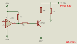
I am trying to detect High side current control with LM339.
I think I should use Scheme1 to reduce the comparator's output to the level of the mictocontroller.

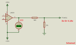
However, since I use a lot of this process in my project, I'm thinking of using the Scheme2 style in order to both take up less space on the card and not have extra delays.
I am aware that the output of the LM339 in schematic 2 is not a pull-up resistor. I'm also undecided whether the absence of this resistor would be a downside for the LM339. Because it says in the datasheet that the output current should be Min.6mA, but while researching, I found many example schematics designed with 500uA (5v/10k). I'm a little confused about this too.

The LM339 datasheet says "Output voltage max.36v" but in my application it produces a voltage of around 281v.
Although there is a lower value (36v x 20mA=720mW == 281v x 0.3mA=85mW) in terms of power, unfortunately I am not educated enough to decide whether this usage will cause problems.

Can I have your opinion on this please

If it is not applicable, if it can be made usable with minor changes, I would be happy if you could help.

Thinking that I can benefit from the zener diode, I also thought of using a 270V zener diode in series with the 1M5 resistor in Scheme1, but I gave up because I could not find it in a small size.
 

Attachments

  • Schema1-2.png
    Schema1-2.png
    17 KB · Views: 143
  • Schema2.png
    Schema2.png
    17.3 KB · Views: 151

Hi,

The schematic without bjt does not work at all, thus let's focus on the one with bjt. It may work.

A comparator has no dedicated GND pin, thus indeed it does never know that 300V exist.
So if all voltages at the comparator are within it's supply rails everything is fine.

300V ... and MCU ... often is a bad combination. Consider to galvanically isolate (according safety regulations) the MCU circuit from the high voltage circuit. You talk about delay... then a high ohmic path in combination with stray capacitance will create some delay.

"Output current 6mA" .. just means it can drive at least (worst case) a load with 6mA. So 6mA and less is fine.

"Output voltage 36V" ... with respect to what? The datasheet should tell. Most probably with respect to the negative supply pin.

Your power calculation: does not apply for the comparator since it never sees a high voltage difference wrt the supply pins. It rather relates to the high ohmic resistor.

Zener is no good solution.

****
Why high side sensing? Isn't there a return path in the low side?
Why not using isolated current sensing?
Show the complete schematic.
Tell us your timing requirements in values with units.

Klaus
 

Schema2 can't work, the simulated voltage of 281V is fake, result of an incorrect comparator model. The output voltage is clamped to negative supply rail by substrate diode, respectively the MCU input will be always high.
 

Hi,

The schematic without bjt does not work at all, thus let's focus on the one with bjt. It may work.

A comparator has no dedicated GND pin, thus indeed it does never know that 300V exist.
So if all voltages at the comparator are within it's supply rails everything is fine.

300V ... and MCU ... often is a bad combination. Consider to galvanically isolate (according safety regulations) the MCU circuit from the high voltage circuit. You talk about delay... then a high ohmic path in combination with stray capacitance will create some delay.

"Output current 6mA" .. just means it can drive at least (worst case) a load with 6mA. So 6mA and less is fine.

"Output voltage 36V" ... with respect to what? The datasheet should tell. Most probably with respect to the negative supply pin.

Your power calculation: does not apply for the comparator since it never sees a high voltage difference wrt the supply pins. It rather relates to the high ohmic resistor.

Zener is no good solution.

****
Why high side sensing? Isn't there a return path in the low side?
Why not using isolated current sensing?
Show the complete schematic.
Tell us your timing requirements in values with units.

Klaus

Thank you for your attention.

Since I do not have a diagram describing my entire project, I had only drawn and shared the relevant part before. I am sharing the full version of the design I planned below.

"Why high side sensing? Isn't there a return path in the low side?"
There is also sensing on the low side. But since the sinus time is very long (15..35mS), I want to detect on the high side so that it is not damaged in case of any short circuit.

By the way my project is AC Inverter

"Why not using isolated current sensing?"
Unfortunately, the high costs of not using something like TMCS1101 for isolated current session.
Since there are 8 three-phase motors in my project, it creates a serious cost in total. In addition, since I have to have it specially brought from abroad in the country I live in, the unit cost remains quite high.

I have no clear information about how long IGBTs can withstand short circuit, but I believe that if I turn off my outputs in a time under my target <1uS, I will not have a problem.
 

Attachments

  • Schema-4.png
    Schema-4.png
    36.9 KB · Views: 113

Schema2 can't work, the simulated voltage of 281V is fake, result of an incorrect comparator model. The output voltage is clamped to negative supply rail by substrate diode, respectively the MCU input will be always high.
Thank you for your attention

You are right.

But what appears there is +281V, VIN+ > VIN-, that is, if the output of the comparator is logical 1, here is the table I calculated. Here is a diagram I drew to draw attention to the situation that will occur at the output of the comparator between the negative feed of the comparator due to the GND coming from the 22k + 1M5.

Since the output of the comparator will be set to +285 when VIN- > VIN+, the value appearing as +281v will already be around 0v.

Since my purpose here is VIN+ > VIN-, 0v from GND with 22k, In the case of VIN+ < VIN-, the result of dividing 285v from the output of the comparator over 1M5 + 22k was to get a result of around 4.2V.

It looked like it could work to me

I was thinking that my problem is that in case of VIN+ > VIN- I cannot decide whether the 281V voltage generated between the output of the comparator and its negative supply will damage the comparator.
 

Hi,

there are cheaper solutions than the TMCS chip. From Allegro or LEM and others...

IGBT (over-) current behaviour usually is given in it´s datasheet.
1us for the full signal chain with a 1.3us comparator is a bit unrealistic. ;-)

Klaus
 

Hi,

there are cheaper solutions than the TMCS chip. From Allegro or LEM and others...

IGBT (over-) current behaviour usually is given in it´s datasheet.
1us for the full signal chain with a 1.3us comparator is a bit unrealistic. ;-)

Klaus
"IGBT (over)current behavior is usually given in the datasheet."
The datasheet of the IGBT I use is at this link. I couldn't find which part is about overcurrent behavior. can you help?

"1us for the full signal chain with a 1.3us comparator is a bit unrealistic. ;-)"
I meant 1uS except comparator :D
I don't know if it would be enough to say <2uS in total. If I find the section about the behavior in the datasheet, I will be enlightened on many issues :)

Is there a situation that you see negative in this scheme?
 

Attachments

  • Schema-4.png
    Schema-4.png
    36.9 KB · Views: 117
Last edited:

Hi,

please in future provide (and use) datasheets directly form the manufacturer. They are most up to date, no advertisement, less likely to contain malware.

Check datasheet: Fig. 11: SOA Characteristics.

I even guess 2us is a bit optimistic.

CD4068? really? Why no 74HC(T)30 --> 10 times faster, cheaper, more modern..

Or why not combine all low side comparators to one input (wired AND) and combine all high side comparators?
A schmitt trigger input won´t hurt...

Schematic: (my saying: a schematic without capacitors is no schematic) bypass capacitors on all power supplies and all REF signals.
The bjt has a specification of 300V absolute maximum. So if you are just for 1 microsecond at 300.01V you are off specification. It is the absolute edge. I don´t recommend this. Also the small distance between 300V pins gives no safety margin.

The 1.5M Ohms resistor needs to be rated for (more than) 300V "Continous operating voltage" .. not 300V short time overvoltage.... and not 300V isolation voltage. Especially at DC when you get one tiny arc aross it, it may not self distinguish the arc. --> fire.
Check datasheet on this.

PCB layout will have big impact on safety and reliability.

Klaus
"Check datasheet: Fig. 11: SOA Characteristics."
I am grateful

I am aware that the CD4068 is very slow compared to the 74HC(T) family. That's why I first built it on top of the 74HC4078 (8 Input OR GATE). I even bought 4-5 to use in my tests.
However, when I was looking for the smd version of this product, when I learned that it was discontinued, I realized that I was in need of the CD family and was disappointed.
Thanks to you, I learned about the existence of the 74HC(T)30. If you think of my disappointment when I learned that I was dependent on the CDxxx family while making nS calculations, you can imagine what a joy it was to learn about the 74HC(T)30.


"please in future provide (and use) datasheets directly form the manufacturer"
You are absolutely right.
I prefer to use only the site that I have given the link of, as I have very, very hard to find on the manufacturer's page.
For example, you can't imagine how many times I've searched for the 74HC4078 on motorola's own page, I still can't find it.

"A schmitt trigger input won´t hurt..."
I think you suggested the schmitt trigger instead of the 74HCT00 in the new schematic. But I can't comment as I don't know the difference between them.

I started my design with an opamp instead of a comparator. So I was entering the ADC inputs of the microcontroller in parallel with the inputs of the 74HC4078. Thus, I would see the phases that do not draw current.
Later, when it switched from opamp to comparator, that architecture remained the same.
Now that you said it, I realized it. all outputs of comparators are open collector, why don't I use it that way???


Finally, I still couldn't determine anything clearly in reading the high side. If pull-up is not mandatory at the output of the LM339, can I use it this way?
 

Attachments

  • Schema-5.png
    Schema-5.png
    67.6 KB · Views: 106

Hi,

Motorla 74HC4078:
I don´t know how many years Motorola does not produce logic ICs anymore. So I doubt you can buy a new motorola 74HC4078. Currently ST seems to still produce them...and provide a datasheet. Simple to find.

Thanks to you, I learned about the existence of the 74HC(T)30
You need to improve your internet search skills.
You are not looking for something like xx4078 or it´s replacement.
--> Just do an "8 input NAND gate" search.

Schmitt trigger:
--> Internet search skills ;-)
It´s used with somehow slow signals or in noisy environment. It just ensures very clean switching .. including hysteresis.
(Again: it´s not urgent to use schmitt trigger here)

pull up is not mandatory:
Who said that? In which context?

Your new circuit:
* low side is fine
* high side won´t work. It is a step back to schematic 2 fo post#1, where we already know it does not work.

BTW: is this a simulation tool that you use?
If not, please do so. And do basic tests on your own.

Klaus
 

Hi,

Motorla 74HC4078:
I don´t know how many years Motorola does not produce logic ICs anymore. So I doubt you can buy a new motorola 74HC4078. Currently ST seems to still produce them...and provide a datasheet. Simple to find.


You need to improve your internet search skills.
You are not looking for something like xx4078 or it´s replacement.
--> Just do an "8 input NAND gate" search.

Schmitt trigger:
--> Internet search skills ;-)
It´s used with somehow slow signals or in noisy environment. It just ensures very clean switching .. including hysteresis.
(Again: it´s not urgent to use schmitt trigger here)

pull up is not mandatory:
Who said that? In which context?

Your new circuit:
* low side is fine
* high side won´t work. It is a step back to schematic 2 fo post#1, where we already know it does not work.

BTW: is this a simulation tool that you use?
If not, please do so. And do basic tests on your own.

Klaus
Since 4078 would not be found, I returned to 4068.

"Just do an "8 input NAND gate" search."
That's how I already found the CD4078i and CD4068. I didn't look at all of them as I thought there was only one product code. I should have kept going through other search results.

I know roughly about the Schmitt trigger. But how to use it here, what are the advantages / disadvantages, I have never experienced. That's what I meant when I said I don't know, I'll keep researching

As for pulling up, I thought it was necessary when I thought about the phrase "output currrent min.6mA", which is used in all schemes and that I mentioned at the beginning.

I am not at the level to interpret the reason why the high side is not working on the schematic, so it seems I need to implement it and work on it.

Thank you for your help.
 

Hi,

"output currrent min. 6mA"
read it as: "the comparator can drive at least 6mA.
This means it´s risky to draw more than 6mA. But it´s safe to draw less.

For the output to become HIGH you need a pullup current. At 15V you may use a resistor of 2.5 kOhms or higher.

***
Simply use a BJT like in post#1 or post#4.

***
Use a simulation software.

Klaus
 

Not sure I followed what your are doing, but the short answer to your posted question is that yes, any voltage on the output of a LM339 over it's maximum rating will cause a problem (likely a zapped LM339).
 

Hi,

"output currrent min. 6mA"
read it as: "the comparator can drive at least 6mA.
This means it´s risky to draw more than 6mA. But it´s safe to draw less.

For the output to become HIGH you need a pullup current. At 15V you may use a resistor of 2.5 kOhms or higher.

***
Simply use a BJT like in post#1 or post#4.

***
Use a simulation software.

Klaus
Hi,

read it as: "the comparator can drive at least 6mA.
This means it´s risky to draw more than 6mA. But it´s safe to draw less.

I guess I must still be misunderstanding. I understood that when it was at least 6mA, I had to draw more than 6mA.
I even perceive it as recommending 16mA by writing Min.6mA typ.16mA in the datasheet.
But in your writings, you say that less than 6mA is safer. I draw less current anyway, it means no problem.

I had questions on how to use it here as I thought the Schmitt trigger only moves within a certain range.
But when I learned the op-amp version, I understood.
The noise factor wasn't very important to me as a single trigger was enough, but it will be very useful since it's 0.3<1.3 ;-)

I am using proteus 7.7 SP2 for simulation. Unfortunately, the LM339 library is not available in it.
But even if it had a library, I don't think it would warn me about what I asked at the beginning.

Thank you for all your help.

Tarik
--- Updated ---

Not sure I followed what your are doing, but the short answer to your posted question is that yes, any voltage on the output of a LM339 over it's maximum rating will cause a problem (likely a zapped LM339).
hi

thank you for your attention

I was thinking if there is no need for a pull-up resistor, can I use it like this?

My aim is;
When VIN+ < VIN-, the +285V voltage from the comparator output is clipped by 22k after passing over 1M5, with 4.xV and logical 1,
When VIN+ > VIN-, I was planning to get logical 0 with GND from 22K, since nothing will come from the output of the comparator.

My question was, if the output of the comparator is idle when VIN+ > VIN-, the +280v voltage between the GND coming from the 22K + 1M5 and the negative supply of the comparator will cause a problem.
Of course, this also applies to VIN+ < VIN-

I had read in the comparator's datasheet that this voltage should be max.36v, but I wasn't sure if I understood it correctly.

I understand that this would be a big mistake

Tarik
--- Updated ---

Hi,

please in future provide (and use) datasheets directly form the manufacturer. They are most up to date, no advertisement, less likely to contain malware.

Check datasheet: Fig. 11: SOA Characteristics.

I even guess 2us is a bit optimistic.

CD4068? really? Why no 74HC(T)30 --> 10 times faster, cheaper, more modern..

Or why not combine all low side comparators to one input (wired AND) and combine all high side comparators?
A schmitt trigger input won´t hurt...

Schematic: (my saying: a schematic without capacitors is no schematic) bypass capacitors on all power supplies and all REF signals.
The bjt has a specification of 300V absolute maximum. So if you are just for 1 microsecond at 300.01V you are off specification. It is the absolute edge. I don´t recommend this. Also the small distance between 300V pins gives no safety margin.

The 1.5M Ohms resistor needs to be rated for (more than) 300V "Continous operating voltage" .. not 300V short time overvoltage.... and not 300V isolation voltage. Especially at DC when you get one tiny arc aross it, it may not self distinguish the arc. --> fire.
Check datasheet on this.

PCB layout will have big impact on safety and reliability.

Klaus
Schematic: (my saying: a schematic without capacitors is no schematic) bypass capacitors on all power supplies and all REF signals.
The bjt has a specification of 300V absolute maximum. So if you are just for 1 microsecond at 300.01V you are off specification. It is the absolute edge. I don´t recommend this. Also the small distance between 300V pins gives no safety margin.

The 1.5M Ohms resistor needs to be rated for (more than) 300V "Continous operating voltage" .. not 300V short time overvoltage.... and not 300V isolation voltage. Especially at DC when you get one tiny arc aross it, it may not self distinguish the arc. --> fire.
Check datasheet on this.

Hi,


When I read your comments here again, I perceive that you do not recommend bjt.

Also, the fact that the KSP92 is max.300v is a separate problem, I guess.


Edit: I reposted the picture for @crutschow. I hope it doesn't cause confusion when the comments are together
 

Attachments

  • Schema2.png
    Schema2.png
    17.3 KB · Views: 91
Last edited:

Hi,
I guess I must still be misunderstanding. I understood that when it was at least 6mA, I had to draw more than 6mA.
Let´s compare it with a bungee rope.
If the information says it can carry 60kg ... 160kg.. it does not say you need put 60kg on it.

You may put 10kg on it and it will safely work.
Put 60kg on it and it will work in either case.
Put 160kg on it and it will work, but not under all conditions. (it will not break, but it may stretch too long)
Put more than 160kg on it and it may probably not work.

****
Schmitt trigger:
A schmitt trigger does not move. What exactly do you mean?
And a schmitt trigger is something completely different to an OPAMP.

***
Proteus:
I don´t use Proteus, but I would be surprised if it does not support one of the most standard comparators.
And:
Don´t expect it to warn you.
But still you can feed it with some input and see what the output is.
Like with the "non bjt" circuits it should show the circuit output always HIGH, independent of the input.
So it´s rather simple to see that the circuit does not do what you expect / does not work at all.

***
When I read your comments here again, I perceive that you do not recommend bjt.
This is completely wrong. Why do you think so? Did I write something wrong?

--> I recommend to use a BJT. But I also recommend to use a suitable BJT with appropriate V_CE specification.

Klaus
 

Hi,

Let´s compare it with a bungee rope.
If the information says it can carry 60kg ... 160kg.. it does not say you need put 60kg on it.

You may put 10kg on it and it will safely work.
Put 60kg on it and it will work in either case.
Put 160kg on it and it will work, but not under all conditions. (it will not break, but it may stretch too long)
Put more than 160kg on it and it may probably not work.

****
Schmitt trigger:
A schmitt trigger does not move. What exactly do you mean?
And a schmitt trigger is something completely different to an OPAMP.

***
Proteus:
I don´t use Proteus, but I would be surprised if it does not support one of the most standard comparators.
And:
Don´t expect it to warn you.
But still you can feed it with some input and see what the output is.
Like with the "non bjt" circuits it should show the circuit output always HIGH, independent of the input.
So it´s rather simple to see that the circuit does not do what you expect / does not work at all.

***

This is completely wrong. Why do you think so? Did I write something wrong?

--> I recommend to use a BJT. But I also recommend to use a suitable BJT with appropriate V_CE specification.

Klaus
Hi,

I think a little differently I guess.
For example, if it says 60..160kg at the bungee station, I think that it is not safe for someone weighing less than 60kg to get on it, thinking that it will fly around with the effect of the wind.
but here I clearly understood that using less than 6mA would not be a problem :)

Since the input voltage ranges of the schimith trigger are fixed (I think it's called VT+,VT-), I couldn't figure out how to use it in my project.
However, in my research, I learned about how the opamp and the schmit trigger were designed.
Example at this link

There is LM339 library in new versions of Proteus, the version I use does not support it because it is not up to date.

Although it's hard to find a to92 or sot23 case where I live, I'll go with a bjt of Vce > 300 :)

Tarik
 

Hi,
Since the input voltage ranges of the schimith trigger are fixed (I think it's called VT+,VT-),
The the "input range" usually more likely is 0.3V beyond supply rails. Datasheet gives exact specification
and VT are the threshold levels, where the logic changes state.
Where do you see the problem with using schmitt trigger inputs in your project? I don´t understand.

Are you sure you still refer "schmitt trigger" to logic ICs (as I meant it in post#8 and you referred to in post#9)
like 74HC(T)14, 74HC(T)132...

BTW: the video (and other videos of this content creator) are not very prefessional, often not complete ... and partly even wrong. It is not the best choice of video.
Better use videos provided or supported by semiconductor manufacturers, universities or professionals with good reputation. Sadly there are a lot of bad videos around.

An OPAMP is meant for analog output, never hitting the rails, never saturated output.
A comparator is meant for digital output, usually always saturated.
Thus a professional would use a comparator when (self) designing a comparator with hysteresis (what they and many other call a Schmitt trigger). A professional won´t use an OPAMP unless it clearly specified for saturated output and specified for big input voltage difference.
While you can always use a comparator you can not always use an OPAMP.

This does not mean that every "opamp made Schmitt trigger" never can work. It may even work with a lot of standard OPAMPS. It depends on the operting condition. Some OPAMPs may fail with modified temperature, modifed supply voltage, modified common mode input voltage, big differential input voltage (it may even burn an OPAMP) and it may cause timing problems.

Klaus
 

Hi,

The the "input range" usually more likely is 0.3V beyond supply rails. Datasheet gives exact specification
and VT are the threshold levels, where the logic changes state.
Where do you see the problem with using schmitt trigger inputs in your project? I don´t understand.

Are you sure you still refer "schmitt trigger" to logic ICs (as I meant it in post#8 and you referred to in post#9)
like 74HC(T)14, 74HC(T)132...

BTW: the video (and other videos of this content creator) are not very prefessional, often not complete ... and partly even wrong. It is not the best choice of video.
Better use videos provided or supported by semiconductor manufacturers, universities or professionals with good reputation. Sadly there are a lot of bad videos around.

An OPAMP is meant for analog output, never hitting the rails, never saturated output.
A comparator is meant for digital output, usually always saturated.
Thus a professional would use a comparator when (self) designing a comparator with hysteresis (what they and many other call a Schmitt trigger). A professional won´t use an OPAMP unless it clearly specified for saturated output and specified for big input voltage difference.
While you can always use a comparator you can not always use an OPAMP.

This does not mean that every "opamp made Schmitt trigger" never can work. It may even work with a lot of standard OPAMPS. It depends on the operting condition. Some OPAMPs may fail with modified temperature, modifed supply voltage, modified common mode input voltage, big differential input voltage (it may even burn an OPAMP) and it may cause timing problems.

Klaus
Hi,

Oh no, I think you are suggesting instead of Schmitt trigger 74HCT30 or CD4068. I commented that you are suggesting instead of LM339. :(

Speaking of noise, I focused on the entry point, the LM339.

I understand now
 

Hi,

Datasheets for LM339 and LM2903, etc., group of comparators show simplified or quite complete schematics of internal structures: NPN open collector or NMOS open drain output.

LM339 output device is an NPN bjt, so a pull-up is necessary for the comparator's high-z output (when In+ < In-) to have a positive voltage.

Surely chancing a PD calculation as the reasoning for violating a voltage-limited device's voltage limit is wonky maths. For example, I'll bet you can't use a CD4000 or SN74xx at 100V and much less at 300V so long as you limit the current to a tiny amount.

When In+ > In-, the comparator will try to sink current by becoming a low impedance path to 'ground'. The internal open collector NPN will ideally only have (I_Rpull-up x R_ce) voltage across its emitter-collector - will that be what the datasheet says to expect (a few hundred mV at most) or will the 40V to 60V maximum Vce of the internal NPN get fried by trying to sink 300V?

Which begs the next question: If your idea works, and only a few mV to a few hundred mV develop across the internal NPN and no voltage spikes damage it, where will the other 299.9V disappear to, or not disappear?

Last, Schmitt triggers, whatever, bla bla bla, and the supposed confusion and a somewhat frivolous attitude - hysteresis, hysteresis, hysteresis... put some hysteresis on the comparators, it's easy to understand why, for God's sake, man! If you don't know what hysteresis is, here's a quick introduction:

Figures 3 and 4

Has a calculator and brief explanation
 

Status
Not open for further replies.

Part and Inventory Search

Welcome to EDABoard.com

Sponsor

Back
Top