Continue to Site

Welcome to EDAboard.com

Welcome to our site! EDAboard.com is an international Electronics Discussion Forum focused on EDA software, circuits, schematics, books, theory, papers, asic, pld, 8051, DSP, Network, RF, Analog Design, PCB, Service Manuals... and a whole lot more! To participate you need to register. Registration is free. Click here to register now.

does datasheet of transistor mention its saturation point?

Status
Not open for further replies.

PG1995

Full Member level 5
Joined
Apr 18, 2011
Messages
248
Helped
1
Reputation
2
Reaction score
1
Trophy points
1,298
Activity points
3,758
Hi

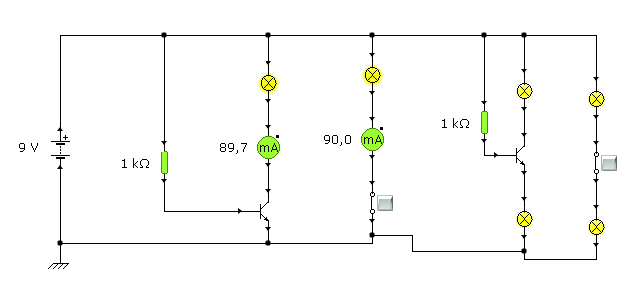
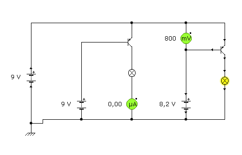
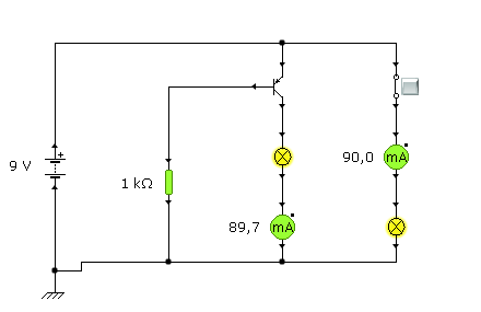
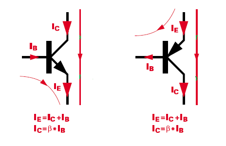
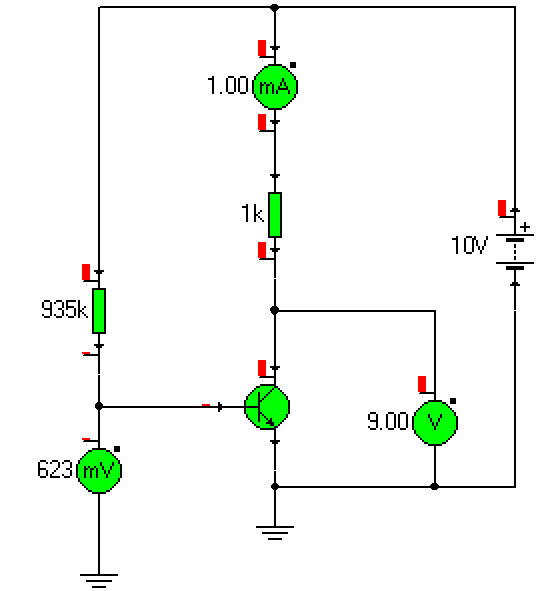
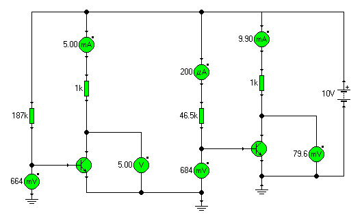
I wanted to if the saturation point of one transistor varies from another. I think it does which would mean every different make of a transistor has a difference saturation point and the datasheet includes it as one of the characteristics. Please let me know. Thank you.

Regards
PG
 

The saturation voltage is called "VCEsat" on the data sheet.

There is a small residual resistance in the transistor junction that make VCEsat rise slightly if more current is made to flow so you will usually see the current at which the voltage was measured is shown as well. In FET devices the saturation voltage is decided by the 'on' resistance of the drain to source channel so you see it referred to as "rds" instead.

Brian.
 

There are no laws that tell a manufacturer what to write to his datasheets. You should refer to datasheets of specific parts.

A term "saturation point" doesn't make sense in my view, because saturation voltage is current dependent. Some datasheets have curves containing this information.
 

Thank you, Brian, FvM.

I'm little confused as usual!:smile:. BJT uses current to control the current flow through collector to emitter while FET uses voltage instead. Saturation point is reached when the flow of current through collector to emitter is at its maximum and no more current could be drawn by increasing the current(BJT)/voltage(FET) at the base. So, would you please tell me why you both have specifically used the term "saturation voltage"? Thank you for the help.

Best wishes
PG
 

Hi,
Current is dependent on voltage value, as you increase the Voltage on Base the current will increase but you have to follow the Safe Area working specifications of a device. You can not overload the device beyond the manufacturer's specifications.
 

Saturation is reached when increasing the base current no longer makes the transistor conduct any more, in other words it has reached maximum conduction between collector and emitter. The letters VCEsat are an abreviation of "Voltage Collector to Emitter at SATuration". Transistors are not perfect though, imagine there is a small resistor in-line with the collector pin, even when the junction is fully conducting there is a small voltage drop across the resistor and by Ohms law a voltage is dropped across it. It means that even when saturated, the collector to emitter voltage will still rise as the current between them increases. That's why VCEsat is specified at a particular current.

You can think of a FET as being a variable resistor between drain and source pins. The voltage applied between the gate and source wil set the resistance between drain and source. Even at minimum value there is still a small resistance present, it never goes down to absolute zero. That's why FETs are specified as having 'Rds' or "Resistance between Drain and Source" rather than saturation voltage. A lower Rds generally means the drain to source voltage will be lower for a given drain current.

Brian.
 
  • Like
Reactions: PG1995

    PG1995

    Points: 2
    Helpful Answer Positive Rating
Datasheet don't give as any information about saturation point (sometimes datasheet gives us such informations figur2 ).
The only information we have is that if we force base current will be equal to
Ib = Ic/10 then the BJT for sure will be in saturation region.
Most BJTs saturation specs are defined saturation when Ic/Ib (called forced beta) = 10.
https://elenota.pl/pdf/ON_Semiconductor/p2n2222a-d.pdf (figure 11)

Normally saturation entirely depends on the BJT current gain β (Hfe) and resistors value Rb and Rc.


For example in this circuit:


β =100
Base current is equal:
Ib=(10V-0.623V)/Rb=10uA
And collector current:
Ic=β*Ib=100*10uA=1mA
And the last emitter current
Ie=Ib+Ic=1.01mA .
Collector current flow through the Rc and causes voltage drop on a resistor.
VRc=Ic*Rc=1V So collector voltage will be equal:
Vce=Vcc-Vrc=9V
If now we change Rb to Rb=187KΩ know we get:
Ib=(10V-0.65V)/187kΩ=50uA---->Ic=100*50uA=5mA
VRc=5mA*1KΩ=5V
Vce=10V-5V=5V
Now it can be seen that if we increase Ib (Vbe increas) ->Ic is increase too, and collector voltage (Vce) also decreases. And that why we say that CE amplifier gives 180 degree phase shift.

Now we can wonder, what is the max Ic that can flow in this circuit.
We knows Ohms law, so Ic_max=Vcc/Rc=10mA and that give as Ib_max=Ic_max/β=100uA
But if we force larger base current the BJT will enter the saturation region

Lets check what will happen if we force the base current equal to Ib=200uA (Rb=46.5KΩ)
And the collector current Ic=100*200uA=20mA
VRc=1KΩ*20mA=20V
and collector voltage
Vce=10-20V=-10V
Of course Ohms law and kirchhoff law must hold.

So Ic can not be greater then Ic_max(Vcc-Vce(sat))≈10mA and Vce=Vce(sat)=0.1V; Ie=Ib+Ic=200uA+10mA=10.2mA and this "state" is called saturation.
So transistor is in saturation when (Rc/Rb)<β_min

But if we remove Rc resistor the saturation will not occur.

 
Last edited:
  • Like
Reactions: PG1995

    PG1995

    Points: 2
    Helpful Answer Positive Rating
Thank you, Raza, Brian, Jony. Special thanks to Brian and Jony for your detailed replies though I would need to read them several times to really understand them.

On a side note, I was thinking that in case of BJT current flows from collector to emitter and collector lies at the top while FET employs opposite convention where the source (equivalent of 'collector') lies at the bottom and drain (equivalent of 'emitter') lies at top. Why is so? Would you please tell me? Perhaps, it's just the way it is without any particular reason. Thank you.

Regards
PG
 

No, the drain in FET is equivalent of the BJT collector and source is equivalent of emitter.

As for the saturation, you must remember that this is up to you as a designer to choose BJT operation point in saturation region.
Simply by forcing Ib > Ic/Hfe_min for a given load current. So in practical case Rb < Rc*Hfe_min.
 
Last edited:
  • Like
Reactions: PG1995

    PG1995

    Points: 2
    Helpful Answer Positive Rating
No, the drain in FET is equivalent of the BJT collector and source is equivalent of emitter.

As for the saturation, you must remember that this is up to you as a designer to choose BJT operation point in saturation region.

I'm so sorry I reversed it. I went through this **broken link removed**, which says "It is a voltage−controlled device in which current flows from the SOURCE terminal (equivalent to the emitter in a bipolar transistor) to the DRAIN (equivalent to the collector). A voltage applied between the source terminal and a GATE terminal (equivalent to the base) is used to control the source − drain current."


I often make embarrassing blunders! :cry: But the good thing is this gives me an opportunity to see the world from a different angle which still have good people, such as many members here, who are always willing to help others and that too without expecting anything in return. I offer my thanks.

Best wishes
PG
 

Here you have some simply explanation how BJT work

To open NPN transistor you need to forward bias the base-emitter junction. Voltage on the base must be larger then voltage on emitter for about 0.6V.
If NPN transistor is full on (saturated) then he act just like a short (switch).
Short collector to GND. Or in general shot collector to emitter.


We get similarly situation in PNP BJT. But this time to open PNP transistor the voltage on a base must be lower (0.6V) than emitter voltage. Or emitter voltage must be higher (0.6V) then base voltage.


And again when PNP is saturate (full on) then he act like switch and shorts emitter with collector. But this time PNP short collector to the Vcc

49_1250871911.png


And this picture will help the intuition
96_1250754356.png


  • Like
Reactions: PG1995

    PG1995

    Points: 2
    Helpful Answer Positive Rating
Hi again, Jony, :)

I hope you won't mind me asking another related question which should have asked before.

As the symbols are drawn current for NPN BJT flows from top (collector) to bottom (emitter). In this case it makes sense because it exactly reflects what the words "collector" and "emitter" mean. PNP BJT is just the reverse case of NPN and in this case of current flows from bottom (emitter) toward top (collector). I think they didn't rename the bottom to 'collector' and the top to 'emitter' in case of PNP to show that it's just reverse of NPN.

Does there exist two reverse types of a FET? I don't think there exist. There exist only one type of FET in which current flows from bottom (drain) to the top (source). So, why didn't they call the "drain" source and the "source" drain? Because this way it would have linguistically made more sense.

I hope you I'm not too much verbose! ;-)

Best wishes
PG
 

As the symbols are drawn current for NPN BJT flows from top (collector) to bottom (emitter). In this case it makes sense because it exactly reflects what the words "collector" and "emitter" mean. PNP BJT is just the reverse case of NPN and in this case of current flows from bottom (emitter) toward top (collector). I think they didn't rename the bottom to 'collector' and the top to 'emitter' in case of PNP to show that it's just reverse of NPN.
Note that arrow on a BJT (on a emitter) symbol show how current will be flow through BJT.
Of course this is conventional current flow (from a higher potential to a lower potential).

In reality in NPN BJT we have "electron" current witch from flow from "-" emitter to " +" collector (negative charge current).
And in PNP we have "hole current" which flow from "+" (emitter) to "-"(collector) (positive charge current).
So in NPN emitter emits electrons, and in PNP the emitter emits holes.

Does there exist two reverse types of a FET? I don't think there exist. There exist only one type of FET in which current flows from bottom (drain) to the top (source). So, why didn't they call the "drain" source and the "source" drain? Because this way it would have linguistically made more sense.
In general we have four types of FET transistors.

The first commercial available field-effect transistors (FET's) were described as junction FET's (JFET).
So we have N-channel JFET and P-channel JFET .
P-channel JFET are very very rare transistors.

34_1316552646.png


After the JFET's another very similar family of field-effect transistor ware developed- the insulated-gate FET (IGFET), which are widely referred to as metal-oxide-semiconductor FET MOSFET.

54_1316553043.png


And we also have N and P channel MOSFET.
N-channel MOSFET are similar to NPN.
And P=channel MOSFET are similar to PNP

And we have two types of a MOSFET family:

depletion-mode MOSFET

enhancement-mode MOSFET

But in real life we only use enhancement-mode MOSFET.
So you don't have to bother your self about other types of the MOSFET.


In all FETs transistor Id = Is
 

Attachments

  • MOSFET.rar
    3.9 KB · Views: 60
Last edited:
  • Like
Reactions: PG1995

    PG1995

    Points: 2
    Helpful Answer Positive Rating
No, the drain in FET is equivalent of the BJT collector and source is equivalent of emitter.

As for the saturation, you must remember that this is up to you as a designer to choose BJT operation point in saturation region.
Simply by forcing Ib > Ic/Hfe_min for a given load current. So in practical case Rb < Rc*Hfe_min.

Hi again,

Okay. The drain in FET is equivalent of collector of the BJT and its source counterpart of BJT's emitter. But isn't it linguistically little confusing? The word "source" implies that the origin of something and "drain" implies drawing off something. So, wouldn't it have made more sense if the drain of FET was called its source and its source was called drain. Do you get what I'm saying? I hope so. Please help me with it. Thank you.

Regards
PG
 

It's mostly just convention. For example, before electricity was less well understood than it is now, it was thought that current flows from positive to negative. Later it was discovered that electrons flow from negative to positive. In practice, it often doesn't really matter which way curent actually flows. When we explain the function of an electronic circuit and say that current flows from this point to that point, it is often more convenient to describe it as flowing from a higher positive point to a lower positive point.
 

Pg, Let me add here a little. AS THE FLOW OF ELECTRONS IS ELECTRIC CURRENT. The very first definition of Electric Current and the electrons carry the Negative charge.
There must an excess point to push the electrons away from the point causing flow of electric current, so many methods are available to make one point to higher side (not discussing here). NOW THE POINT IN EXCESS OF ELECTRONS is said to be the POSITIVE with reference to QUANTITY. This is said to be POSITIVE (in quantity not the charge) and naturally the flow is from Higher side (Positive in Quantity) to lower side (Negative in Quantity). This was interpreted by the non familiar people to electricity which finally created a confusion.
I think I could make a little explanation in simple words to understand.
 
Last edited:

Status
Not open for further replies.

Similar threads

Part and Inventory Search

Welcome to EDABoard.com

Sponsor

Back
Top