halisimon
Newbie level 4
irfs4610
Hi All.
I was trying to develop a two stage inverter (DC-AC) with a half bridge on the primary side of the flyback transformer.
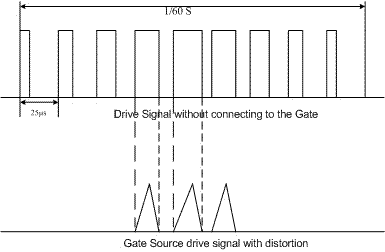
As shown in the figure 1, each switch on the upper and lower rail operates half cycle which is defined at the line frequency(60Hz). Moreover, the switch at each half cycle will turn on and off at 40Khz which is modulated by PWM signal, on the other hand, the other switch will stay OFF during the whole period until the other half cycle comes.
I hooked up the drive circuit and measured the output signal on the LO (since the lower output return is defined as the common ground and high output return haven't been connected yet), the output drive signal is perfect with the amplitude 15V.
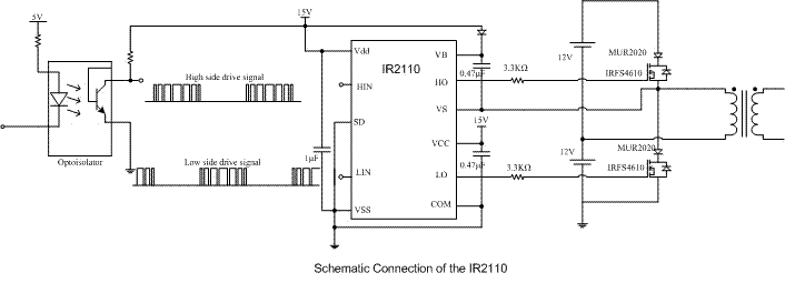
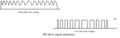
However, when I connected the low and high output to the Gates of the MOSFET as shown in thr schematic diagram. The gate-source voltage which is supposed to be the real drive signal presents a serious distortion as shown in the fig 2.
Apparently, the distortion shows some charging and discharging phenomenon of the capacitor, I am not sure is this because of the Miller effect in the MOSFET or the outside capacitor which is connected between the VB and VS.
The IR2110 is designed to drive the MOSFET directly and MOSFET is 'voltage control' device, I really don't think something wrong with the Gate current. or issue on the drive capability
Anyone met this kinds of problem before? I need a solution to get rid of the distorton.
Thanks alot, everybody.
Hali-Simon
Fig for distortion 2
Hi All.
I was trying to develop a two stage inverter (DC-AC) with a half bridge on the primary side of the flyback transformer.
As shown in the figure 1, each switch on the upper and lower rail operates half cycle which is defined at the line frequency(60Hz). Moreover, the switch at each half cycle will turn on and off at 40Khz which is modulated by PWM signal, on the other hand, the other switch will stay OFF during the whole period until the other half cycle comes.
I hooked up the drive circuit and measured the output signal on the LO (since the lower output return is defined as the common ground and high output return haven't been connected yet), the output drive signal is perfect with the amplitude 15V.
However, when I connected the low and high output to the Gates of the MOSFET as shown in thr schematic diagram. The gate-source voltage which is supposed to be the real drive signal presents a serious distortion as shown in the fig 2.
Apparently, the distortion shows some charging and discharging phenomenon of the capacitor, I am not sure is this because of the Miller effect in the MOSFET or the outside capacitor which is connected between the VB and VS.
The IR2110 is designed to drive the MOSFET directly and MOSFET is 'voltage control' device, I really don't think something wrong with the Gate current. or issue on the drive capability
Anyone met this kinds of problem before? I need a solution to get rid of the distorton.
Thanks alot, everybody.
Hali-Simon
Fig for distortion 2
") IanP, actually, the resistor i use is 1K, still too big, isn't it? I will try to hook it up with smaller one as you mentioned tomorrow.
IanP, actually, the resistor i use is 1K, still too big, isn't it? I will try to hook it up with smaller one as you mentioned tomorrow.