Continue to Site

Welcome to EDAboard.com

Welcome to our site! EDAboard.com is an international Electronics Discussion Forum focused on EDA software, circuits, schematics, books, theory, papers, asic, pld, 8051, DSP, Network, RF, Analog Design, PCB, Service Manuals... and a whole lot more! To participate you need to register. Registration is free. Click here to register now.

diode in diode connected MOS

Status
Not open for further replies.

kavitha_rapolu

Junior Member level 3
Joined
Jan 4, 2008
Messages
26
Helped
0
Reputation
0
Reaction score
0
Trophy points
1,281
Activity points
1,460
What is the purpose of diode in this circuit?


Keep Vdg ~= 0.7v and in saturation region, I guess.
 

I think this diode will make the NMOS gate can be charged fast and discharged much slowly.
 
Can you explain how diode will help NMOS gate to be charged up fast and discharged slowly?
 

If this was (say) an ESD clamp, the shunt FET would have a good
"hang time" beyond where the load has discharged below a useful
Vgs.

But I would never use such a structure, its lack of "turnoff authority"
on the gate is too much uncertainty to put in my circuits.
 

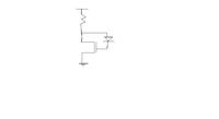
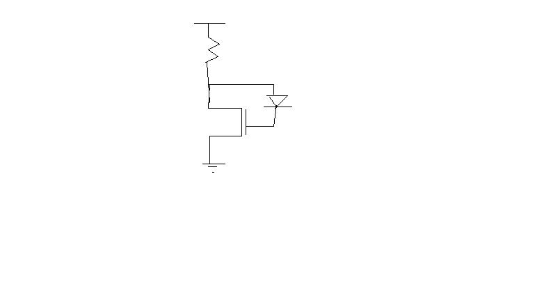
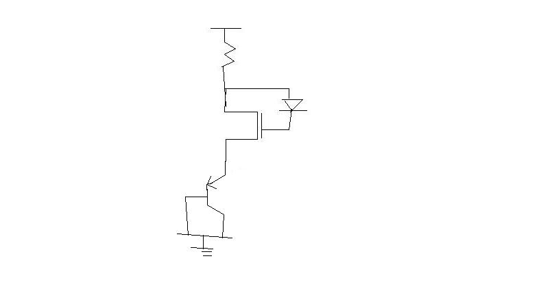
here nmos Vd = Vgs + Vdiode & we are getting this 'vd' for less ckt bias current 'id'
this can be done by increase length of nmos, but may be you are gaining some area due to square law dependency of Vgs with id in saturation
 

It could not be ESD clamp because it will have current leakage always.
If this was (say) an ESD clamp, the shunt FET would have a good
"hang time" beyond where the load has discharged below a useful
Vgs.

But I would never use such a structure, its lack of "turnoff authority"
on the gate is too much uncertainty to put in my circuits.


---------- Post added at 06:09 ---------- Previous post was at 06:05 ----------

The NMOS gate is charged up fast by the current flowing from the supply, resistor and the diode. So the charging path will decide the NMOS turn-on time.
On the other hand, when supply is off, NMOS gate can't be discharged thru the diode. It can be discharged very slowly thru gate current leakage.
Can you explain how diode will help NMOS gate to be charged up fast and discharged slowly?
 

Thank you. what is the purpose of this circuit? ie having PNP transistor at the bottom?
 

Status
Not open for further replies.

Similar threads

Part and Inventory Search

Welcome to EDABoard.com

Sponsor

Back
Top