Continue to Site

Welcome to EDAboard.com

Welcome to our site! EDAboard.com is an international Electronics Discussion Forum focused on EDA software, circuits, schematics, books, theory, papers, asic, pld, 8051, DSP, Network, RF, Analog Design, PCB, Service Manuals... and a whole lot more! To participate you need to register. Registration is free. Click here to register now.

differential signal spacing and current bus shielding?

Status
Not open for further replies.

prcken

Advanced Member level 1
Joined
Nov 1, 2006
Messages
419
Helped
41
Reputation
82
Reaction score
37
Trophy points
1,308
Location
Shanghai
Activity points
4,059
Hi,

I am wondering in the layout for high speed (> 10 GHz) differential signal, what's the spacing is reasonable? the signals will deteriorated a lot by the mutual capacitance?

Another question about the layout of a bus of current sources in the chip (schematic shown below), for example, i have more than 20 current sources go to different places on chip, should I use ground shielding for the currents?
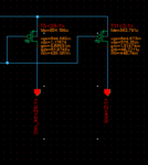
Capture.PNG

Thanks!
 

... in the layout for high speed (> 10 GHz) differential signal, what's the spacing is reasonable? the signals will deteriorated a lot by the mutual capacitance?

If the signals are really good differential signals (same driver, same slew rate, same load), you may route them with min. spacing. That's the idea and meaning of using differential signals. An additional advantage is minimal coupling to crossing signals.

... about the layout of a bus of current sources in the chip (schematic shown below), for example, i have more than 20 current sources go to different places on chip, should I use ground shielding for the currents?

I've never shielded DC current sources - their essential usage is DC bias. If you have very long wires, you could think of adding a single (poly) cap to GND, if there's an (otherwise) unused space nearby.
 

I have found that even at much lower frequencies, spacing
wants to be well above minimum if your differential signal
has far to go. Just the mutual capacitance vs the driver
strength at 400MHz made me push differential spacing to
10um between, 10um clearance to other lines, and periodic
crossover-flips to balance the loading where the lines ran
parallel to power bussing for thousands of um.

Extracted capacitance was showing me these issues.
 

Another question about the layout of a bus of current sources in the chip (schematic shown below), for example, i have more than 20 current sources go to different places on chip, should I use ground shielding for the currents?

Distributing biasing by current isn't a good idea. Much better is to distribute gate voltage through whole chip
 

Distributing biasing by current isn't a good idea. Much better is to distribute gate voltage through whole chip

Depends: if you can get a (P)VT-independent current delivered from a central high-precision BGR controlled current reference, this can make your life (design) a lot easier.
 

Gate voltage distribution of strongly degenerated cascode current sources for global biasing is in my opinion better option. But of course I never did any research to proove this ;-)
 

....An additional advantage is minimal coupling to crossing signals

Why it has minimal cross coupling with minimal spacing? to my understanding, the smaller the spacing, the larger the mutual cap, thus will introduce more coupling. Am I right?

- - - Updated - - -

Gate voltage distribution of strongly degenerated cascode current sources for global biasing is in my opinion better option. But of course I never did any research to proove this ;-)

if the current is large, there may have significant voltage drop along the ground bus so that the gate-source voltages could be very different from what was intended. that's my concern.
of course by distributing gate bias will save lots of power and easy layout.
 

of course by distributing gate bias will save lots of power and easy layout.
It's a considerations about distance induced transistor mismatch and PSRR influence for crosstalk (mainly in multichannel design).
Erikl rightly noticed that it depends ;-)
 

....An additional advantage is minimal coupling to crossing signals

Why it has minimal cross coupling with minimal spacing? to my understanding, the smaller the spacing, the larger the mutual cap, thus will introduce more coupling. Am I right?

This is a misunderstanding, Prcken, sorry: The meaning is: you get minimal clock coupling to (orthogonally) crossing signal lines, because the simultaneous rising and falling edges of both differential clock signals cancel each other re. the coupling effect to the crossing signal line.
 

Status
Not open for further replies.

Part and Inventory Search

Welcome to EDABoard.com

Sponsor

Back
Top