Continue to Site

Welcome to EDAboard.com

Welcome to our site! EDAboard.com is an international Electronics Discussion Forum focused on EDA software, circuits, schematics, books, theory, papers, asic, pld, 8051, DSP, Network, RF, Analog Design, PCB, Service Manuals... and a whole lot more! To participate you need to register. Registration is free. Click here to register now.

Differential Pair Design

Status
Not open for further replies.

Dididito

Newbie level 5
Joined
Sep 5, 2011
Messages
10
Helped
0
Reputation
0
Reaction score
0
Trophy points
1,281
Activity points
1,368
Hello everybody,

This is my first post in the forum. I hope I can learn as much as possible from all of you, and help you when you need it.

I'm starting right now on IC design, I would like to desing a Two Stages OpAmp. With a differential pair in the first stage.

The differential pair I'm using as reference has two PMOS as input and two NMOS as active load. I'm using AMS 0.35um technology.

My problem is that the output of the differential pair is saturated, and I really don't know how to solve it. Any idea or advice??

Thank you very much in advance.
 

My problem is that the output of the differential pair is saturated
What do you mean with this?Transistors fall into linear region?
Explain further...or show a transient plot.

Did you check the biases in the whole circuit and are correct at the desired point?The desired point is determined by your specifications.
 

Any idea or advice??
Yes. Show your circuit with power supply and bias circuitry.
 
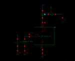
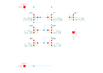
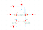
Sorry, I forgot to show the schematics and the plots. Here they are:

schematic.pngschematic2.pngsnapshot.png

You can see the result of the simulation, as well as the schematic of the differential pair and the schematic used to simulated it.
 

1.)You have not biased the gates of MN0,MN1...You should either use an ideal Vdc initially or more correctly get this bias potential from a current mirror.
2.)The two branches of the differential pair are not symmetrical! (I see deviations to their currents)
3.)As fas as your tail current Ibias is concerned this method is not correct to model the real transistor that will be used there...you should use a transistor model there, that is the ideal Idc in parallel with an ideal resistanse,the latter will model fet's small-signal output resistanse.In this way you can fix the potential at the sources node of MP1,MP3.
4.)Your diff pair's input DC level is 0V?Are you sure that this is in your ICMR?
 
I have been checking all the points you have mentioned.

1) I have used now a current mirror to bias. (Check Image).
2) I was changing some parameters and in the image I upload the parameters where different between both branches, now both are equal.
3) I think that now that I'm using a real current mirror I won't need that resistance right?
4) The signal that I'm using at the input are both 0.5 amplitude, 100 Hz and initial phase 0 and 180 respectly.

As you can see, not it's less saturated, but anyway, I'm not getting as high gain as I desired.

I really appreciate your help and your time in advance, thank you very much to understand it better.

schematic.png
schematic2.png
snapshot.png
 

No using the current mirror you are ok.No need for resistanse.
You are using too high signal at your inputs...1V differential is too high i think.The input signal should be determined by your specs.
Anyway try to inject some mV at your inputs and see what's going on at the output.
Also,fix your input common mode.I don't think that 0V is a "good" idea.Usually we bias the input in the middle (Vdd-Vss)/2,Vdd/s for your case since Vss=0.
In any case,you will decide which is the most suitable point for your design.
 
Once again, you were right, the input signal were too high.

I did a quickly test circuit to test the differential pair and I didn't think about it. Now it's not getting saturated and it's having a reasonable good gain. (check image)

Anyway I have some others question:
1) I want to use a common-source stage after this one, should I correct offset in the pair, in the common-source, or in both of then??
2) How can I get a accuracy control of the gain in the differential pair?

Thank you soooo much!!! :D

snapshot.png
 

You mean the Vos offset voltage?Since you will make use of a second stage you must measure the offset totally via monte carlo simulations.
Remember the definition of Vos.It is the differential input voltage that you must apply in order to force your output become 0 (for symmetrical/dual power supplies).If you have single supply the quiescent point of your output is in most cases at Vdd/2.So,since your output is after the second stage,then you must simulate this effect totally in your design.

What do you mean by saying "accuracy control"?Explain this phrase further according to your goal.
 
Ok then, I understand what you meant about Vout offset. I'm going to try to simulated and to correct the offset by myself and if I have some troubles I will let you know.

Related to accuracy control of the gain. I mean which parameters should I take into account in order to modify the gain as I want. If I'm not wrong, the gain of the differential pair will be: Av=gm(P1)*(rds(P3)||rds(N1)). Where P1 and P3 means the P-Channel Transistors 1 and 3 (see image above) and N1 N-Channel (active load).

It means that changing the bias current I would be able to increase the gain and also increasing W of transistors and decreasing L. Are there some others terms I'm forgotting??
Thank you very much in advance again.
 

Correct,based on the equation you wrote that gives the DC gain of your diff. pair stage you can play with the various parameters (Ibias,Vgs of the input pair,W,L etc.) and reach a desired gain.It is quite easy whith the aid of some trial and error simulations.Go on and if you need more help don't hesitate to ask again.
 
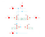
Well, I have been trying to modify some parameters in order to obtain a good output voltage (including the second stage we were talking before). As you can see in the image, I have again a saturated output.

As I told you, I am a rookie in IC design, so I really don't know what should be the minimun length for the transistors? In my case (I'm using 0.35um technology) I am using 0.7 um for all transistors, both P and N channel; and usually for PMOS I use 3 times the width of NMOS transistors. I don't know if that is correct (maybe not).

Besides, I would like to have as minimum current consumption as possible.

Perphaps because of your experience you could give some other advice.

schematic.pngsnapshot.png
 

Forget the transient output signal at the moment.
Try to bias and size your transistors in a way that all are in saturation and you reach your specs (mainly the gain,transit frequency,phase margin,ICMR and output swing).
You can refer to some tutorials from Google (like **broken link removed**) or read some basic analog books (Gray-Meyer,Razavi,Allen-Holberg etc...) and see
how things work.Don't waste a lot of time in bibliographic research,just get a good perception of how it's parameter affects your performance and then play with the simulator to achieve your goals.
In this way you have a good theoritical background and an intuitive perception of your design as an IC engineer.

The final transient test should contain a sinus input source with amplitude=max. input signal (given from your specs) and if you notice clipping or distorion then you should revise your linearity and output swing goals.

As i see now,transistors MN4,MN5 in your schematic are not biased...use an ideal Vdc there or a current mirroring.
 
Last edited:
I will check all those points then. But why did you say that MN4 and MN5 are not biased?? I see 627mV at the Gate, it should be enough to bias the transistor, isn't it??

Thank you very much for help and info. You has helped me a lot, and I have learn quite much about IC design.
 

Hello jimito13,

I have been checking the tutorial that you have recommend me, it's quite useful, I'm learning how to play with the parameters in order to obtain my goals.

But there is something in the tutorial that I don't understand. In the page 17, it sais that:
Vsd5(sat)=Vsg5-Vtp=Vdd-Vbias-Vtp0

How can I get Vbias?? Is a value that you fix in order to be sure that the transistores is bias??? Or you get it from some other equation???

Thank you very much again.
 

As you should know and written in many books,for older uμ-scale processes and for long channel devices the drain-source voltage for which the FET enters the saturation region is given by the equation :

Vds,sat=Vgs-Vt

Now according to the schematic of the tutorial because the M10 fet is diode connected it is in effect that : Vgs(M5)=Vgs(M10)=Vg(M10)-Vs(M10)=Vd(M10)-Vdd=Vbias-Vdd.

Combine those two equations and you have the result.You should also manipulate the modulus signs for this case because your transistor is pmos and the above equations are written for nmos device (i selected this for simplicity).

Vbias is the drain potential of the M10 transistor and is created by the Ibias flow.In a real implementation Ibias consists of a resistor or a transistor or both of them.So,in this way via the resistor and the current flowing there you can
control this voltage.
 

Yes I knew the equation that gives the saturation region.

I did the analisys that you did about how get Vgs.

My question was about how can I get Vbias. I guest that it was created by the Ibias flow. But my question refers that, in case that I don't know the dimensiones (W,L) of M10 yet. I guess if I fix the vbias, then the dimensions where directly proportional to Vbias. I mean, I can fix vbias and the I will obtain a value for W/L ratio. Am I right???

Thank you for your help and for your time.
 

I think i already answered to your question...read more carefully my previous post.
Anyway,i describe briefly the procedure :

You must first define the proper (the one that fits your needs/specs) bias voltage at the gate of M5,thus you have Vbias.
Secondly you will decide (if not given from specs) what Ibias current you want to mirror to each inner branch of your opamp and with this value given you will size your transistor (W/L) accordingly to allow the flow of Ibias.
Finally,you should fix the resistor value by ohm's law : R=(Vbias-Vss)/Ibias=Vbias/Ibias since Vss=0.

That's all the story!
 
Ok, I understand.

I didn't understand in your previous post because I was confuse due to what I really know from my specs is the Ibias, not Vbias.

Now, I have understood that I fix Vbias in order to fit that M5 must be bias.

Thank you and excuse me.
 

Status
Not open for further replies.

Part and Inventory Search

Welcome to EDABoard.com

Sponsor

Back
Top