Continue to Site

Welcome to EDAboard.com

Welcome to our site! EDAboard.com is an international Electronics Discussion Forum focused on EDA software, circuits, schematics, books, theory, papers, asic, pld, 8051, DSP, Network, RF, Analog Design, PCB, Service Manuals... and a whole lot more! To participate you need to register. Registration is free. Click here to register now.

Designing single stage Operational Trans conductance Amplifier using TSMC 180nm

Status
Not open for further replies.

anandsrivas

Newbie level 4
Newbie level 4
Joined
May 30, 2013
Messages
7
Helped
0
Reputation
0
Reaction score
0
Trophy points
1,281
Location
INDIA
Visit site
Activity points
1,342
Designing single stage Operational Trans conductance Amplifier for bio amplifier for recording the(Action potential and local field potential) neural signals using TSMC 180nm technology.
Design:-The design of OTA is shown below. we have to determine
• The transfer function
• The required width and length ratio of transistors ,value of bias current ,vdd according to the tsmc 180 nm technology.

After designing OTA in gateway (silvaco) and assigning values of (w/l),vdd, Ibias .Then Transient analysis, AC analysis of the OTA is done to see the results in smartview.
Required parameters:
Supply voltage ,Supply current ,Gain ,Bandwidth ,Lower cutoff frequency ,High cut off frequency,Input referred noise ,CMRR ,PSRR,noise efficiency factor.
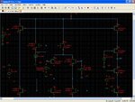
180nm based OTA.JPG180nm based OTA 1.JPG

- - - Updated - - -

I ned urgent reply please help to complet my project plz help
 

Attachments

  • 180nm based OTA.bmp
    2.3 MB · Views: 140

Refer to **broken link removed** for Phiilip Allens notes. Just take the lectures on Opamps. The procedure for design is given there along with equations.

With a few iterations you can adapt it to your design.
 
  • Like
Reactions: Fabien

    Fabien

    Points: 2
    Helpful Answer Positive Rating
Designing single stage Operational Trans conductance Amplifier for bio amplifier for recording the(Action potential and local field potential) neural signals using TSMC 180nm technology.
Design:-The design of OTA is shown below. we have to determine
• The transfer function
• The required width and length ratio of transistors ,value of bias current ,vdd according to the tsmc 180 nm technology.

After designing OTA in gateway (silvaco) and assigning values of (w/l),vdd, Ibias .Then Transient analysis, AC analysis of the OTA is done to see the results in smartview.
Required parameters:
Supply voltage ,Supply current ,Gain ,Bandwidth ,Lower cutoff frequency ,High cut off frequency,Input referred noise ,CMRR ,PSRR,noise efficiency factor.
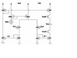
View attachment 91751View attachment 91750

- - - Updated - - -

I ned urgent reply please help to complet my project plz help

Dear anand

It is a little late for me to answer you, I am feeling sleepy right now... any way I will try my best to help you with your thread tomorrow. I already finished designing like this amp

By the way could you tell me about your simulator, i see it is free edition, is it working fine comparing with cadence or mentor ????
 

This simulator is SYMICA it is the full rep[lacement of cadence and all files and every thing we are going to as we use in HSPICE and cadence tool, if possible so please help me in design and simulation result taht i need i don't have any problem with particular simulator i need to complet that as soon with in the week

- - - Updated - - -

Dear anand

It is a little late for me to answer you, I am feeling sleepy right now... any way I will try my best to help you with your thread tomorrow. I already finished designing like this amp

By the way could you tell me about your simulator, i see it is free edition, is it working fine comparing with cadence or mentor ????

This simulator is SYMICA it is the full rep[lacement of cadence and all files and every thing we are going to as we use in HSPICE and cadence tool, if possible so please help me in design and simulation result taht i need i don't have any problem with particular simulator i need to complet that as soon with in the week

- - - Updated - - -

Refer to **broken link removed** for Phiilip Allens notes. Just take the lectures on Opamps. The procedure for design is given there along with equations.

With a few iterations you can adapt it to your design.

Dear Sir,
Thanks for help but I have not so much time left to design again if possible so help me more as you have nay thing point to point related to that I have only this week its the last week for my project finalization
 

Hello,

for the design you have to go through Allen philip book as nith suggested you, the design is that complicated thing, this anther tried his best to make it easy. please refer to this page from that book 298. you need to use the equations presented there. the only different from your design is that he is using resistors, however it will not effect the main equations you need.

As you see, the first starts with selecting the biasing current value based on the slew rate and the GBW value.

keep in your mind that the calculated values are never going to be identical with the simulated values because the calculations are based on a very simplified models and equations. However, it is mandatory that you do and understand the procedure because you are going to modify and change and optimize your design during the simulation.

please if you dont understand any of the steps or if you dont have this book, just tell me.


Designing single stage Operational Trans conductance Amplifier for bio amplifier for recording the(Action potential and local field potential) neural signals using TSMC 180nm technology.
Design:-The design of OTA is shown below. we have to determine
• The transfer function
• The required width and length ratio of transistors ,value of bias current ,vdd according to the tsmc 180 nm technology.

After designing OTA in gateway (silvaco) and assigning values of (w/l),vdd, Ibias .Then Transient analysis, AC analysis of the OTA is done to see the results in smartview.
Required parameters:
Supply voltage ,Supply current ,Gain ,Bandwidth ,Lower cutoff frequency ,High cut off frequency,Input referred noise ,CMRR ,PSRR,noise efficiency factor.
View attachment 91751View attachment 91750

- - - Updated - - -

I ned urgent reply please help to complet my project plz help

- - - Updated - - -

Hello,

for the design you have to go through Allen philip book as nith suggested you, the design is that complicated thing, this anther tried his best to make it easy. please refer to this page from that book 298. you need to use the equations presented there. the only different from your design is that he is using resistors, however it will not effect the main equations you need.

As you see, the first starts with selecting the biasing current value based on the slew rate and the GBW value.

keep in your mind that the calculated values are never going to be identical with the simulated values because the calculations are based on a very simplified models and equations. However, it is mandatory that you do and understand the procedure because you are going to modify and change and optimize your design during the simulation.

please if you dont understand any of the steps or if you dont have this book, just tell me.


Designing single stage Operational Trans conductance Amplifier for bio amplifier for recording the(Action potential and local field potential) neural signals using TSMC 180nm technology.
Design:-The design of OTA is shown below. we have to determine
• The transfer function
• The required width and length ratio of transistors ,value of bias current ,vdd according to the tsmc 180 nm technology.

After designing OTA in gateway (silvaco) and assigning values of (w/l),vdd, Ibias .Then Transient analysis, AC analysis of the OTA is done to see the results in smartview.
Required parameters:
Supply voltage ,Supply current ,Gain ,Bandwidth ,Lower cutoff frequency ,High cut off frequency,Input referred noise ,CMRR ,PSRR,noise efficiency factor.
View attachment 91751View attachment 91750

- - - Updated - - -

I ned urgent reply please help to complet my project plz help
 

Dear Sir,
Sorry , i don't have that book and all so please if possible so send me that book and as well as please give detail. my mail id anandsri85@yahoo.co.in. I need the reply urgent last 3 day left for me

Hello,

for the design you have to go through Allen philip book as nith suggested you, the design is that complicated thing, this anther tried his best to make it easy. please refer to this page from that book 298. you need to use the equations presented there. the only different from your design is that he is using resistors, however it will not effect the main equations you need.

As you see, the first starts with selecting the biasing current value based on the slew rate and the GBW value.

keep in your mind that the calculated values are never going to be identical with the simulated values because the calculations are based on a very simplified models and equations. However, it is mandatory that you do and understand the procedure because you are going to modify and change and optimize your design during the simulation.

please if you dont understand any of the steps or if you dont have this book, just tell me.


- - - Updated - - -

Hello,

for the design you have to go through Allen philip book as nith suggested you, the design is that complicated thing, this anther tried his best to make it easy. please refer to this page from that book 298. you need to use the equations presented there. the only different from your design is that he is using resistors, however it will not effect the main equations you need.

As you see, the first starts with selecting the biasing current value based on the slew rate and the GBW value.

keep in your mind that the calculated values are never going to be identical with the simulated values because the calculations are based on a very simplified models and equations. However, it is mandatory that you do and understand the procedure because you are going to modify and change and optimize your design during the simulation.

please if you dont understand any of the steps or if you dont have this book, just tell me.

- - - Updated - - -

Any one give full circuit with all voltage and current value in my circuit apply for 180 nm technology so please help me as soon a possible, that forum support is my last hope i have only 3 days ledt plz help me

Dear Sir,
Sorry , i don't have that book and all so please if possible so send me that book and as well as please give detail. my mail id anandsri85@yahoo.co.in. I need the reply urgent last 3 day left for me
 

Hello Sir,
thanx for that help but still there is one more problem is that we are don't now about the value of currents and W/L values, the bias voltages VNB1, VNB2 and VPB2 so how we give that value

use this one, lecture 240 page 8
 

Dear SIr,

i am still wating for some final ans and no result are getebale for me if you have any idea so plz help and send the spice net list file for me
 

You need to use the equations in the notes/book mentioned above to find the values of W/L for all the transistors. To set the bias points you need to set up a biasing circuit. Just Google for it.

I have a feeling that you don't even know the µn, µp and Cox values of the MOS transistor equation. You need to find out that first by doing some basic simulations.

- - - Updated - - -

This thread might help with your issues.
 
Last edited:

Dear Anand,

If you have Skype - we can discuss the design methodology, it should take approximately one hour tops if you are unfamiliar with the design procedure. This is a simple OTA with cascoded output.

You should Ideally provide the following parameters;

Vdd
GBW
Gain (dB)
Slew Rate (V/us)
Mobility N and P devices, in uA/V2
Cox
Sub threshold slope, n
Lambda (for calulating Rds)

Threshold Voltage.

My Skype account is Kenneth.Potter4

Let me know if you would like to discuss...

- - - Updated - - -

Anand,

Just one more point, if your parameter values are from a specific PDK then please supply these in private when we discuss your design as they will be under a non disclosure agreement so do not post them on the forum.

Regards, Ken.
 

it is nice idea to make skype contact, i would take part of it

please give me your skype address to add you
 

Hi Junus,

My Skype address was given in my previous post, again it is Kenneth.Potter4

Can you let me know what you would like to discuss as my post was to answer questions regarding Anand's problem.

Regards, Ken.
 

Status
Not open for further replies.

Part and Inventory Search

Welcome to EDABoard.com

Sponsor

Back
Top