Continue to Site

Welcome to EDAboard.com

Welcome to our site! EDAboard.com is an international Electronics Discussion Forum focused on EDA software, circuits, schematics, books, theory, papers, asic, pld, 8051, DSP, Network, RF, Analog Design, PCB, Service Manuals... and a whole lot more! To participate you need to register. Registration is free. Click here to register now.

Designing LC filter for power converter

Status
Not open for further replies.

samEEEf

Full Member level 2
Full Member level 2
Joined
Apr 17, 2010
Messages
133
Helped
1
Reputation
2
Reaction score
1
Trophy points
1,298
Visit site
Activity points
2,197
I've found two equations in two different books to determine the required inductance for a LC filter.
Marty Brown - Power Supply Cookbook (2nd Edition) - [p.46, Eq. 3.32]
Lmin=(Vinmax-Vout)*Toff/(1.4*Iout)

Switching Power Supply Design, Third Edition - [p.74, Eq. 2.20]
Lo=0.5*Vo*T/Ion

Which equation should we consider?


[Reference updated]
 
Last edited:

There are many filters out there with different orders. I think Lmin differs from L0. Lmin is the least inductance needed for the filter to be a filter. L0 points out the typical L for that filter.
 

Let the parameters -
Vinmax=380v
Vout=Vo=325v
Iout=Io=1A
T=20us (for frequency 50KHz)
Toff= 7us (not clear about the explanation of the book itself)

So,
Lmin=(380-325)*7/(1.4*1)=275uH

Lo=0.5*325*20/1=3250uH

:sad:
 

If you want anyone to comment the quoted design equations, you would tell page and formula reference numbers...

Apparently both formulas have different prerequisites (e.g. minimal current for continuous mode). They are discussed in the books, but probably not very clearly. Particularly the derivation of the first equation is somehow mysterious, the author seems even to confuse Ton and Toff.

In this siuation, it can be helpful to lay the books aside and make your own calculation based on your design goals. Or chose the convenient way and use a free circuit simulator like LTspice.
 

@FvM:

Reference number updated. Sorry for the inconvenience.

Could you please suggest a reference book to get such an effective formula? I want to make it practically and need to use a good reference too.
 

I prefer the guru Keith Billings who has 50 yrs SMPS design experience and many books.

The choke must not saturate during Ton and must have enough energy stored during Ton so the voltage does not sag during Toff. The ripple current should be not much more than 25% Idc.

Buck Choke Specification (inductor with DC current and AC ripple)

Output voltage Vo.max.
Input voltage Vi.max.
Output DC current Io.max.
Max. ripple current e.g. 20% of Io.max.
Max. temp. rise. 30deg C

During the “off” period, the current falls by 20% of Io.max. ,and for this example, and the inductance may be calculated.

During the “off” period, current loop B is established, and the magnitude of the voltage across the choke, |e|, is the output voltage plus the diode voltage drop (the diode, being forward biased) & the current is flowing in diode loop under the forcing action of choke L1. During this period the current will be decaying at a constant rate defined by Vout+Vdiode=e (across coil)

The ripple voltage depends when switch is on.

Duty ratio = t.on/T= Vout/Vin =325/380=85.5%.

since
t.on + t.off = T , the PWM on & off


e =L dI/dt where dI is ripple current and dt =t.off when switch is off
And e=Vout +Vf.diode ~Vout

Read book for more details. Starting page 477 of 849 ,
Switchmode_Power_Supply_Handbook_3rd_ed
 

Actually I was trying to know about designing LC filter for Bridge converter. I found some choke design guideline for Buck converter in Switchmode_Power_Supply_Handbook_3rd_ed as referred.
Need the calculation of required inductance and capacitance for a bridge converter.
 

Confused
Am I checking wrong thing :sad:

at p 476
1.9 DESIGN EXAMPLE OF CHOKES FOR BUCK
AND BOOST CONVERTERS (BY AREA PRODUCT
GRAPHICAL METHODS AND BY CALCULATION)

This section continues to p 478

Could you please refer the section name and number?
 

Yes that was the general area.

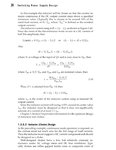
Here is another one of his books. Source : Switching Power Supply Design, Third Edition Abraham I. Pressman, Keith Billings, Taylor Morey, Copyright © 2009 by The McGraw-Hill Companies 807 pages.

I will only show 1 page of the book, I suggest you buy it.

It is based on the equation of matching Volt-seconds when the switch is on to when off and current loop is supplied by the clamp diode.
Where V=L dI/dt thus Volt-seconds = L dI


It shows a continuous mode Buck with only 10% ripple current, or you can choose 20% ripple, but the more ripple, the bigger the choke or less margin to saturation.

There are too many alternative configurations to generalize, but this is the basic concept.

image.jpg
 

Okay, but what about the following equations -

f=1/(2*pi*sqrt(LC))

If the switching frequency of a bridge converter is 50kHz, we can make a LC filter considering cutoff frequency less than the switching frequency (say 40kHz in this case). By selecting a convenient capacitor value, we'll be able to find the inductor value. Is my understanding correct?
 

The dimensioning of the first level filter chokes in SMPS hasn't much to with LC resonance frequency. They are energy storage elements, the design equations are based to large signal quantities and criteria are like keeping continous conduction mode for a specified minimal current.
 

I found LC filter for DC/DC converter in the following doc (Design tip 7)

**broken link removed**
 

The formula for L in switching converter is based on continuous mode current and maximum ripple of say 10 or 20% as used in my 2nd reference book.

The result may still be excessive voltage ripple for a given load capacitance, so an additional series L is chosen for series mode resonance to notch the switching frequency fundamental ripple voltage using the standard resonant formula as you confirmed in Output LC filter guide.
 

Status
Not open for further replies.

Similar threads

Part and Inventory Search

Welcome to EDABoard.com

Sponsor

Back
Top