imrankhanPNU
Member level 1
Hello!
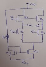
I have done calculations for designing a differential amplifier (DA) with differential output. I simulate (using cadence ) the DA with the calculated values and perform the DC analysis of the circuit to inquire all the transistors are operating in saturation. However, I did not get all the transistors in the saturation region. I tried to tune the system (means to bring it to saturation region) but tuning one set of transistor results in the detuning of other transistors and vice versa.
if someone can review my calculations and suggest me correction. I will be thanked for my help.
Design Parameters:
GBW= 5MHz CL= 10pF, Vdd=5V
UnCox=151u A/V^2;
UpCox=26u A/V^2;
Av= 100
Vtn=0.85V Vtp=-1V
Slew Rate (SR) :5V/uSec
ICMR+= 4V ; ICMR- =1.5V (input Common mode range)
Step 1 _ Calculating Id:
Id=SR*CL 5V/uSec * 10pF= 50uA
Step 2 - Calculating (W/L) for M3 and M4:
Vds1>=Vmax-Vthn=4-0.85=3.15V (let consider it as 3.5V)
Vds3=Vdd-Vds1=5-3.5=1.5V
For M3 to be in saturation:
|Vds3|>=|Vgs3|-|Vthp|
1.5V >= |Vgs3| - 1V
|Vgs3|<= 2.5V (I take |Vgs3| : 2V )
Id3=Id/2 = 25uA
(W/L)3= 2* Id3 / UpCox * (|vgs3| - |Vthp| = 2
Step 3 - Calculating (W/L) for M1 and M2:
gm1=GBW * 2 * pi * CL
= 5M * 2 * 3.14 * 10pF
=314u
Id1=Id/2=25uA
(W/L)=gm1^2 / 2 * Id1 * unCox
(W/L) =13.06
Step 4 _ Calculating (W/L) for M5 and M6:
To keep M1 in saturation under ICMR- (1.5V):
Vin>=Vgs1+Vdsat5
Vgs1=1V (I calculate it as we know Id1=25uA , W1/L1=13.06 )
Putting Vin=1.5 (ICMR-) & Vgs1= 1V
Vdsat5<=0.5V
Id5=Id
(W/L) =2 * Id5 / UnCox * (Vdsat) ^ 2= 2.64
Finally, transistor dimensions are:
(W/L)1,2 = 1.9u / 1u
(W/L)3,4 = 13.06u / 1u
(W/L)5,6 = 2.64u / 1u
