sky_123
Advanced Member level 4

- Joined
- Feb 26, 2011
- Messages
- 1,166
- Helped
- 279
- Reputation
- 566
- Reaction score
- 270
- Trophy points
- 1,363
- Activity points
- 9,606
Hello,
As some may know, KNJN's boards are not open (no circuit diagrams or source code is supplied). I made the mistake
of purchasing a couple of boards a while back, and I'd like to use one for an experiment, but I wanted to get an idea of the circuit.
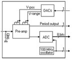
All that is supplied is a block diagram. I'm guessing there is a high speed input buffer amp (FET based), and
some adjustable VSS to provide an offset. I've attached hi-res images of the board if anyone is good at detective
work. The SOT-23 devices hi-res images are also attached in the third image, marked A/B/C/D/E. If anyone can identify any/all of the five devices,
it would be great (I've tried some googled SMD marking sites, but I'm not familiar with any decent sites for this).
There is also a small 5-pin device marked 'SACI' - maybe a serial EEPROM for the DAC settings.


Last edited:
